Silicon Germanium IC´s on the RF Market
A. Schüppen, H. Dietrich, D. Zerrweck, H. v. d. Ropp, K. Burger, N. Gellrich, J. Arndt, M. Lentmaier, B. Jehl, J. Imschweiler, W. Kraus, F. Voswinkel, T. Asbeck, H. Conzelmann, W. Arndt, R. Kirchmann, A. Voigt, and K. Wörner
TEMIC Semiconductors (An Atmel Company), 74072 Heilbronn, Germany
Introduction
Since 1974 the research on SiGe layers was heavily stimulated by the works of Erich Kasper, Ulf König, and Horst Kibbel [1], [2]. The principles of the growth of SiGe and a lot of technology details were invented by researchers of the DaimlerChrysler research center in Ulm, Germany. The break-through for SiGe into production was the first well functioning HBT at the end of the eighties [3]. The 1994 measured 113 GHz transit frequency of a double mesa SiGe-HBT [4] was one of the fastest silicon based devices until 1998 [5]. The 1995 achieved world record of maximum frequency of oscillation with 160 GHz is still valid [6].
In early 1993, U. König and A. Gruhle from Daimler Benz and H. Dietrich at TEMIC started a feasibility study and a predevelopment of SiGe-HBTs [7]. However, the real transfer into production started within the SIGMA project in the beginning of 1996 and was finished two years later in early 1998 [8]. Now SiGe1 is on the market, and a couple of well-known electronics companies are customers of TEMIC’s SiGe1 technology.
Silicon Germanium heterobipolar transistors (SiGe HBTs) offer the opportunity to fabricate high performance ICs for RF systems in the 1 – 10 GHz range. The greatest benefit of SiGe one can earn in analog and mixed signal circuits as e.g. low noise amplifiers (LNAs), power amplifiers (PA), mixers, voltage controlled oscillators (VCOs), and phase locked loops (PLLs). In addition, high frequency analog to digital and digital to analog converters (ADCs and DACs) are reasonable circuits.
The advantages of SiGe over pure silicon for these applications are mainly the extremely high cutoff frequencies with record values from research HBTs of fT = 130 GHz [5] and fmax = 160 GHz [6], and a ECL gate delay down to 9.3 ps [9]. The good high frequency noise performance with rf noise figures of 0.9 dB at 10 GHz [10] emphasizes the potential of SiGe HBTs in mobile communication systems. Furthermore, an important argument for using HBTs for wireless applications is the high power added efficiency at low DC voltages. SiGe HBTs challenge not only silicon, but also GaAs MESFETs by the higher linearity and gain for operation voltages below 3.6 V [11]. The main advantage of SiGe HBTs over III-V HBTs is that a standard Si production line and most of the standard bipolar process modules can be used for device fabrication. This allows low cost production with high yield and excellent reliability.
Technology and DC-Performance
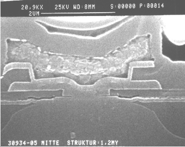
TEMIC offers a production technology, called SiGe1, including npn HBTs with and without selectively implanted collector on the same wafer [12]. The main important issue of the technology is the differential growth of the SiGe layer after a standard recessed LOCOS process. The SiGe poly is used for the base contact and for two of the three resistor types. The emitter has an inside and an outside spacer and an additional alpha-Silicon layer in order to perform the emitter and the collector contact. A SEM cross section of the emitter portion of a HBT is depicted in Fig. 1.
Fig. 1: Cross Section of the emitter part of a SiGe HBT.
In addition, spiral inductors, nitride capacitors, three types of poly resistors, a LPNP, rf- and dc-ESD protection, and varactor diodes are incorporated in the present technology. The parameters of the technology are summarized in Table 1.
In contrast to other companies, as e.g. IBM [13] and Siemens [14], which prefer a triangular Ge profile with only up to 15% Ge in their medium doped base, TEMIC´s SiGe1 technology has a nearly box shaped Ge profile with above 20% Ge in the base. The epitaxy itself is controlled by monitor wafers as depicted in Fig. 4 over three months. The highly boron doped SiGe base, 4x1019 cm-3, which is grown by a single wafer CVD machine, has a real advantage over the drift HBTs due to the approximately 10 times smaller base sheet resistance, revealing values of 1.5 kW /„ . Hence, it is possible to use wide emitter stripes, up to 2 µm, for power HBTs.
The main important parameters of the SiGe1 Technology are collected in Table 1.
|
Parameter [unit] |
non–SIC |
SIC |
|
NPN transistor |
|
|
|
Transit frequency fT [GHz] |
30 |
50 |
|
Max. frequency of oscillation fmax [GHz] |
50 |
50 |
|
Current gain hFE [] |
180 |
180 |
|
Early voltage VA [V] |
50 |
50 |
|
Collector emitter breakdown voltage BVCE0 [V] |
6.0 |
3.0 |
|
Collector base breakdown voltage BVCB0 [V] |
15 |
12 |
|
Noise figure at 2 GHz Fmin [dB] |
1.0 |
1.0 |
|
LPNP |
|
|
|
Collector emitter breakdown voltage BVCE0 [V] |
7 |
|
|
Current gain hFE [] |
7 |
|
|
Typical collector current ICP [µA] |
40 |
|
|
Passive devices |
|
|
|
High ohmic poly resistor (poly1) RH [W /sq] |
400 |
|
|
Medium ohmic poly resistor (poly2) RM [W /sq] |
110 |
|
|
Low ohmic poly resistor (poly1–TiSi2) RL [W /sq] |
4.5 |
|
|
Precision MIM capacitor cSPEC [fF/µm²] |
1.1 |
|
|
Spiral inductor 4 nH, Q–value at 2 GHz Q [] |
7 |
|
|
ESD Zener diode, Zener voltage VZ [V] |
6.2 |
|
|
Zener diode, parasitic capacitance [pF] |
5.5 |
|
|
RF–ESD diode, parasitic capacitance [pF] |
0.3 |
|
Table 1: Summary of the essential parameters of the SiGe1 technology.
Reliability
In order to demonstrate the reliability of the process a couple of important PCM parameters were collected over several lots.
Figure 2 corresponds to the expected probe yield for a chip having about 2000 minimum size transistors integrated. The SiGe1 technology is comparable in terms of masks and costs to a standard double poly Si BJT process. Therefore this technology is well suited for large scale integration (LSI), as nicely demonstrated in Fig. 3, which shows a wafer mapping of the 10k transistor arrays over a typical 6 inch wafer. In addition, a couple of lifetime tests on single HBTs and complete packaged circuits were all positive and were summarized in a special qualification report. The process was recently qualified.
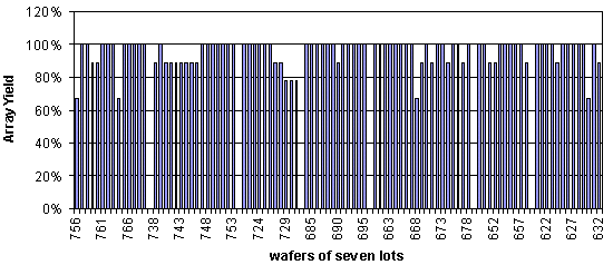
Fig. 2: Yield of PCM transistor arrays, corresponding to 2000 minimum size transistors.
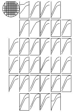
Fig. 3: Wafer mapping of a 10000 HBT array; HBT: 0.8x1.6 µm2; array size: 3.5 mm2.
RF and Noise Measurements
The SiGe HBTs reveal transit frequencies fT of 30 GHz (Fig. 4) with a collector emitter breakdown voltage of BVCEO = 6 V and 50 GHz with BVCEO = 3 V, respectively.
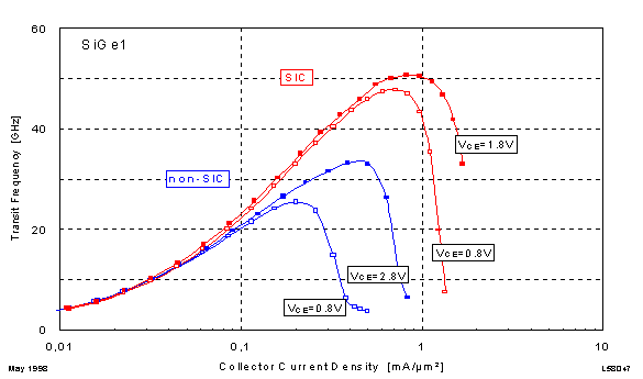
Fig. 4: fT values of single emitter devices with and without SIC.
The maximum fT and fmax values were achieved at current densities of 0.3 mA/µm² and 0.65 mA/µm² for the non-SIC and the SIC devices, respectively (Fig. 4).
For large signal applications, as e.g. power amplifiers, the linearity of the gain over a voltage swing is of great interest. The voltage dependence of the maximum frequency of oscillation and of the transit frequency for the non-SIC HBT revealed a constant value for VCE voltages above 1.5 V. Hence for PAs high PAE values and a good linearity can be expected.
For low noise amplifiers the low high frequency noise of SiGe HBTs in the 1 to 5 GHz range is a real advantage over homo bipolar transistors. The typical minimum noise figure of SiGe1 HBTs at 2 GHz is about 0.8 dB, owing from the low base sheet resistance and the high current gain of 180. The associated gain is in the range of 17 dB.
Power SiGe HBTs
In order to demonstrate the performance of multi finger power devices, HBTs with different numbers of emitter fingers were investigated. The effective size of each finger is 1.6 x 30 µm2.
On each side of the emitter is a base contact in order to achieve a low base resistance, and a collector finger contact is placed between a group of base and emitter contacts. To achieve homogenous current distribution for all emitters, a 4 Ohm ballast resistance is inserted in series to each emitter. The Gummel plot and the output characteristics of the multi emitter finger HBTs show good dc performance. The ideality factor of the base and the collector currents are close to 1 and the current gain hfe is nearly constant over a wide current range. Due to the very high base doping the early voltage is above 50 V. The current gain is in the range of 150 and the breakdown voltage BVCE0 is 6 V, which is well suited for systems with 3.6 V battery power supply. The output characteristics of SiGe HBTs show no offset voltage, which is a big advantage over III-V single heterostructure HBTs, because the offset voltage reduces the efficiency of the HBT in large signal operation.
A 10 emitter device with output matching for the fundamental frequency 1.9 GHz and 3rd harmonic achieved a value of 62% PAE. The results of the 10, 20 and 40 emitter devices show that the power scales with the number of emitters. With these devices 21 dBm, 24 dBm, and 27 dBm have been achieved in class AB operation at a collector-emitter voltage of 3.6 V. The PAE slightly decreases with the number of emitters from 62% at 21 dBm, to 50% at 32 dBm because the gain also decreases with the number of emitters. Gain reduction in multi emitter devices is a consequence of long internal connection lines of the devices. The electromagnetic coupling between these lines is responsible for gain and cut-off frequency reduction. In order to demonstrate the power capability of these HBTs also a 80 emitter stripe HBT was measured at 0.9 GHz showing 32 dBm output power and a corresponding PAE of 50%. Measurements on different geometries, finger lengths, and contact arrangements indicate that a further lateral layout optimization is still possible.
However, the newest results showed that it is possible to achieve PAE values as high as GaAs HBTs achieved at 900 MHz and 1.9 GHz. One of TEMIC’s customers measured power added efficiencies as high as 72% at 900 MHz and 64% at 1.9 GHz as depicted in Figs. 5 and 6 [15] – [17].
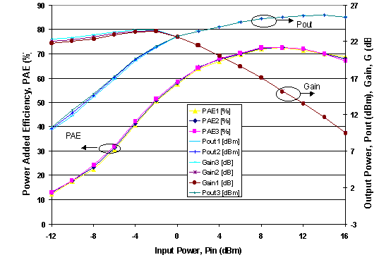
Fig. 5: Large signal results of 20 emitter HBT at 900 MHz revealing 72% PAE.
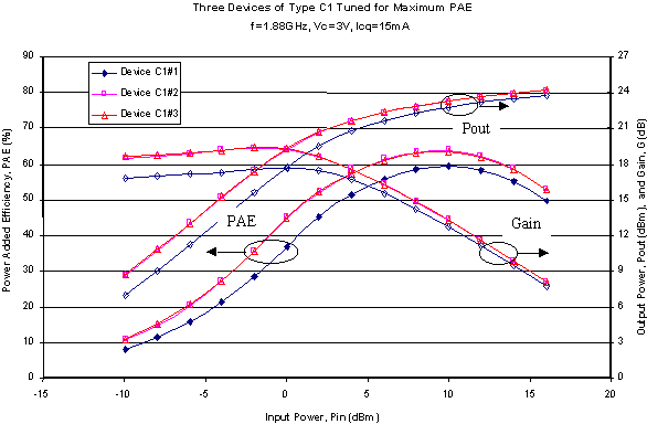
Fig. 6: Load pull measurements of 20 emitter HBT at 1.88 GHz (two different geometries).
Circuits
On research level a couple of SiGe based circuits were investigated in the last few years, e.g. a digital to analog converter (DAC) from IBM in 1993 [18], optical transmitter circuit from NEC in 1994 [19], [20], VCOs at 26 GHz and 40 GHz from Daimler-Benz in 1995 [21].
The application of the SiGe technology will be in wireless communication systems in the 1 – 6 GHz range. Hence, mixers, GSM power modules, dual band front-ends for GSM and DCS 1800 and DECT front-ends are in the focus. Additionally, LNA circuits were designed by the subcontractor University of Ulm and achieved a noise figure of 1.6 dB and an associated gain of up to 26 dB at 5.8 GHz. The relatively small bandwidth of the 5.8 GHz LNA is an advantage for mobile communication systems, reducing the expense for the input filter [22] – [24].
The first commercial product is a DECT front-end including a LNA with 1.6 dB noise figure and 20 dB gain combined with a 27 dBm power amplifier with 41% PAE over the whole packaged device, Fig. 7. This DECT front-end is now in production as one IC of a complete chipset [25].
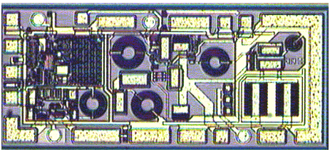
Fig. 7: DECT power amplifier with LNA.
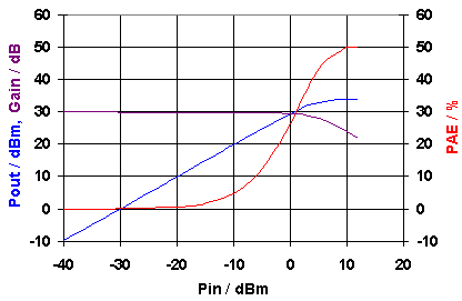
Fig. 8: Output power, power added efficiency and gain vs. input power of a flip-chip GSM-PA.
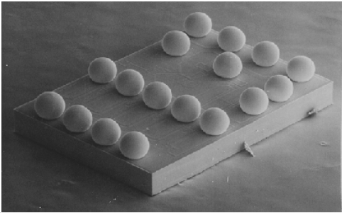
Fig. 9: REM photograph of a flip-chip GSM-SiGe-HBT 3 stage power amplifier.
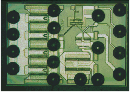
Fig. 10: Top view of GSM PA.
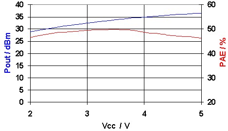
Fig. 11: GSM-flip-chip amplifier; PAE = 50%, Gain = 30 dB, Pout = 32 – 36.5 dBm, Vop = 2 – 5.5 V.
The second SiGe1 product group will be the TST0911, TST0912, and TST0913. These are power amplifiers for dual-band (GSM and DCS 1800) and for GSM and DCS 1800, respectively. Some important pictures and measurements are shown in Figs. 9 – 11. The overall PAE of the whole GSM chip achieves 50% and an output rf power up to 4.5 W. The power of these three stage amplifiers is voltage controlled, in order to set the power level to the needed value. The photographs shows a chip of the GSM amplifier, having approximately 300 emitters, whereas the dual-band IC has about 500 emitter stripes with 1.6 x 30 µm2, corresponding to an emitter area of 18750 minimum size transistors.
Conclusions
Thanks to the differential epitaxy and the SiGe box profile the SiGe1 technology is well suited for analog and mixed signal applications. The real HBT concept distinguished by a high doped base and a lower doped emitter originates from the Daimler Chrysler research center in Ulm and was successfully improved to a production technology in the last three years at TEMIC in Heilbronn. TEMIC´s SiGe1 production technology is a 30/50 GHz fT and 50 GHz fmax technology. It includes besides the two types of npn HBTs three types of poly resistors, nitride capacitors, spiral inductors, DC and RF ESD diodes and lateral pnp transistors.
SiGe1 is used for RF low noise amplifier and power amplifiers in mobile phones, e.g. DECT, GSM, DCS1800, CDMA, TDMA. In addition, gain blocks, dual-band transceivers and mixer circuits for base stations are in the product portfolio.
The quality and the reproducibility of the technology were demonstrated by highlights as functioning 10k arrays over whole wafers and lots, by 0.5 W power HBTs revealing 72% PAE at 900 MHz and 64% at 1.8 GHz, a LNA at 5.8 GHz with a record noise figure of 1.6 dB and 26 dB associated gain, and a 2:1 multiplexer showing a clear eye diagram at 40 Gbit/s.
However the main important message of this paper is:
The first TEMIC SiGe-IC´s are on the market.
References
[1] E. Kasper, H. Kibbel, U. König: Silicon germanium heterobipolar transistor structures with extremely high base doping, Material Research Society Symposium Proceedings 220, 451- (1991)
[2] U. König, M. Kuisl, J.F. Luy, H. Kibbel, F. Schäffler: Differential molecular beam epitaxy for multilayered bipolar devices, Thin Solid Films 184, 253-260 (1990)
[3] P. Narozny, H. Dämbkes, H. Kibbel, E. Kasper: Si/SiGe Heterojunction Bipolar Transistor made by molecular beam epitaxy, IEEE Transaction on Electron Devices 36(10), 2363-2367 (1989)
[4] A. Schüppen, A. Gruhle, H. Kibbel, U. Erben, U. König: SiGe-HBTs with high fT at moderate current densities, Electronics Letters Vol.30(14) (1994), pp. 1187 – 1188
[5] K. Oda, E. Ohue, M. Tabanbe et al.: 130 GHz fT SiGe HBT Technology, IEDM Tech. Dig. (1997), pp. 791 – 794
[6] A. Schüppen, U. Erben, A. Gruhle, H. Kibbel, H. Schumacher, U. König: Enhanced SiGe Heterojunction Bipolar Transistors with 160 GHz-fmax, Technical Digest of the IEDM 95, (1995), pp. 743 – 746
[7] A. Schüppen, H. Dietrich: High Speed SiGe Heterobipolar Transistors, Journal of Crystal Growth 157, (1995) pp. 207 – 214
[8] A. Schüppen, H. Dietrich, S. Gerlach, H. Höhnemann, J. Arndt, U. Seiler, R. Götzfried, U. Erben, H. Schumacher: SiGe–Technology and Components for Mobile Communication Systems, Proceedings of the 1996 BCTM (1996), pp. 130 –134.
[9] K. Washio, E. Ohne, K. Oda, M. Tanabe, H. Shimamoto, and T. Onai: A selective-epitaxial SiGe HBT with SMI electrodes, featuring 9.3 ps ECL gate-delay, Tech. Dig. Int. Electron Device Meeting, 1997, pp. 795 – 798.
[10] Schumacher, U. Erben, A. Gruhle: Low-noise performance of SiGe heterojunction bipolar transistors, Tech. Dig. IEEE MTT-S Int. Microwave Symp., 1994, pp. 1167 – 1170.
[11] U. König, A. Gruhle, A. Schüppen: SiGe Devices and Circuits: Where are Advantages over III/V ?, IEEE GaAs IC Symposium (1995), pp. 14-17
[12] A. Schüppen, H. Dietrich, U. Seiler, H.v.d. Ropp, U. Erben: A SiGe RF technology for mbile communication systems, Microwave Engineering Europe, June (1998), pp.39 – 46
[13] D. L. Harame, J. M. C. Stork, B. S. Meyerson, K. Y.-J. Hsu, J. Cotte, K. A. Jenkins, J. D. Cressler, P. Restle, E. F. Crabbe, S. Subbanna, T. E. Tice, B. W. Scharf, and J. A. Yasaitis: Optimization of SiGe HBT technology for high speed analog and mixed-signal applications, Tech. Dig. Int. Electron Device Meeting, (1993), pp. 71 – 74.
[14] M. Wurzer, T. Meister, H. Schäfer, H. Knapp, J. Böck, R. Stengl, K. Aufinger, M. Franosch, M. Rest, M. Möller, H.-M. Rein, and A. Felder: 42 GHz static frequency divider in Si/SiGe bipolar technology, Tech. Dig. IEEE Int. Solid-State Circuits Conf., (1997), pp. 122 – 123.
[15] U. Erben, M. Wahl, A. Schüppen, H. Schumacher: Class-A SiGe HBT Power Amplifiers at C-Band Frequencies, IEEE Microwave and Guided Wave Letters 5(12) (1995) , pp. 435 – 436.
[16] A. Schüppen, S. Gerlach, H. Dietrich, D. Wandrei, U. Seiler, U. König: 1W SiGe Power HBT’s for Mobile Communication, IEEE Microwave and Guided Wave Letters, Vol.6 (9) (1996), pp. 341 – 343.
[17] U. Seiler, H. Dietrich, A. Schüppen: Load pull analysis of SiGe power HBTs for mobile communication systems, Proceedings of the 28th European Solid State Device Conference (1998), pp. 456 – 459.
[18] P. Xiao, K. Jenkins, M. Soyuer, H. Ainspan, J. Burghartz, H. Shin, M. Dolan, and D. Harame, A 4 b 8 GSample/s A/D converter in SiGe bipolar technology, Tech. Dig. IEEE Int. Solid-State Circuits Conf., 1997, pp. 124 – 125.
[19] T. Hashimoto, H. Tezuka, F. Sato et al.: SiGe Bipolar ICs for 20 Gb/s optical transmitter, BCTM (1994), pp. 163 – 170.
[20] T. Masuda, K.-1. Ohhata, E. Ohne, K. Oda, M. Tanabe, H. Shimamoto, T. Onai, and K. Washio: 40 Gb/s analog IC chipset for optical receiver using SiGe HBT’s, IEEE Int. Solid-State Circuits Conf., (1998), pp. 314 – 315.
[21] A. Gruhle, A. Schüppen, U. König, U. Erben, H. Schumacher: Monolithic 26 GHz and 40 GHz VCOs with SiGe Heterojunction Bipolar Transistor, Technical Digest of the IEDM 95 (1995), pp. 725 – 728.
[22] U. Erben, A. Schüppen, H. Dietrich, H. Schumacher: Low–Noise Amplifier for Mobile Communications Using a Production Ready SiGe HBT Technology, Proceedings of the 27th ESSDERC (1997), pp. 368 – 401.
[23] U. Erben, H. Schumacher, A. Schüppen, J. Arndt: Application of SiGe Hetero junction bipolar transistors in 5.8 and 10 GHz LNAs, Electonics Letters Vol 34, No 15, (1998), pp.1498 – 1500.
[24] W. Dürr, U. Erben, A. Schüppen, H. Dietrich, H. Schumacher: Low-power low-noise active mixers for 5.7 and 11.2 GHz using commercially available SiGe HBT MMIC technology, Electronics Letters, Vol 34, No 21, (1998), pp.1994 – 1996.
[25] R. Götzfried, F. Beisswanger, S. Gerlach, A. Schüppen, H. Dietrich, U. Seiler, K.–H. Bach, J.Albers: RF ICs for mobile communication systems using SiGe Bipolar Technology, IEEE Transactions on Microwave Theory and Techniques 46(6), (1998), pp. 661 – 668.