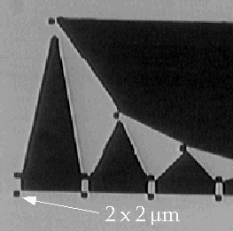
Fig. 1: Sample output of the pattern generator.
In this paper, the main activities in the cleanroom of the MISZ (microstructure center) are described. The cleanroom of the MISZ was opened 1993; during 1994, most of the equipment for the production of semiconductor devices was installed. Since 1995, state of the art growth of III-V compounds as well as the production of patterned masks used in lithography is done on a regular basis. We also give a short description of all projects running in our institute that are involved in the cleanroom. Projects sponsored additionally by the GMe are not described in detail.
One of the main research areas of our institute is the preparation and characterization of III-V devices. Therefore the fke maintains several collaborations with national and international research institutions and companies by providing them with epitaxial layers (III-V-compounds). A second main research topic is the production of micron and sub-micron devices down to nanometer scale. Patterned masks for optical lithography are also provided to different institutions.
Since 1995, the cleanroom of the MISZ is running on a regular basis. Main research areas are the state of the art growth of III-V compounds and the production of patterned masks. Supplementary to the normal operation and maintenance of the cleanroom equipment, an additional wet bench was installed. Testing of the cleanroom quality and adjustment (laminar air flow, filters, cooling, humidity…) if necessary is done periodically.
As additional equipment, a Reactive Ion Etching machine (Oxford Plasmalab 80+) was bought and installed in the cleanroom of the MISZ in 1995. As process media, Ar, O2, SF6, Cl and SiCl4 were installed. The RIE will mainly be used for three projects: the fabrication of nanostructures, surface grating couplers for semiconductor lasers, and GaAlAs selective etching processes for base contact formation in three terminal resonant tunneling devices. For nanostructure fabrication, SiCl4 processes will be employed. At present, the three above processes are optimized to perform the final acceptance tests of the machine as soon as possible.
The Pattern Generator GCA 3600F is a fully automatic instrument to generate circuit patterns in photoresist as well as in high resolution emulsion materials. To achieve best results, however, at present the PG is run exclusively on photoresist-coated masks.
The PG-system includes a 20X-reduction lens with automatic focus motion to compensate for plate wedge, it has two interchangeable light sources for emulsion (flash lamp) and photoresist exposure (Hg-lamp), and a laser metering of X- and Y-stage position over 150 mm of stage motion in each coordinate. The stage position over 150 mm is specified in increments of 0.1 µm. The system has a variable aperture system which provides height, width and angle control of individual rectangular image elements used to generate an arbitrary circuit pattern, an instrument control system and a vacuum plateholder that is capable of accommodating 2.5" through 7"-plates in standard thicknesses from 0.06" through 0.25". The PG is supported by a vibration isolation table and is enclosed in a GCA Environmental Chamber to guard against vibration, temperature change (accuracy of 0.1o) and to ensure an adequate volume of clean temperature controlled air flow across the instrument during operation.
Fig. 1: Sample output of the pattern generator.
The PG is controlled by a DEC PDP 11 series digital controller, a 9 channel, 800 bit per inch, 10.5" reel magnetic tape unit, a system interface controller and a video keyboard terminal. The design of the mask patterns is done in AutoCad. The resulting dxf-files are translated in proper dwm-files by a special software (ASM 2600™ by Artwork Conversion Software). This allows the use of a PC 486 for the data transfer to the PG instead of the magnetic tape. The PG is used to expose patterns on standard photoplates, which are delivered by Hoya Corporation, Japan. A 350 W mercury-lamp is used as the light source. The photoplates are glass plates coated with a 800 Å thick Cr-layer and 500 nm thick AZ 1350 positive photoresist. The flatness of the plates is smaller than 5 µm over the whole plate size. The plate used are either 3.5"-size or 5"-size. The 5"-size are mainly used as master reticles for the photorepeater. The exposed plates are developed, etched with a chromium etch and finally cleaned with a photoresist remover.
The minimum feature size that can be exposed is 2 x 2 µm. The feature size can be increased up to 1300 µm in steps of 0.5 µm. Due to the useful conversion software the PG allows basically the generation of arbitrary patterns, rectangles, triangles and even circles, as is demonstrated in Fig. 1.
The GCA 3696 Photorepeater (PR) is a fully automatic instrument capable of exposing a 22 mm square image area on photoresist coated plates or directly on photoresist-coated wafers. A 5X g-line reduction lens (Zeiss Maximum 1000) permits the minimum feature size to a line width of 0.9 µm. System software allows conversational input dialogue to reduce errors and simplify specification of the system and the job to be exposed.
A laser position transducer with automatic compensation for atmospheric conditions and work piece temperature is employed to meter X- and Y-stage positioning over a 150 mm x 150 mm square exposable area. The system includes a matched illumination system with a 350 W mercury lamp, an automatic focus, a computer, and a video keyboard terminal. Like the PG, the PR is also supported by a vibration isolation table and is enclosed in a GCA Environmental Chamber.
5"-photomasks that were exposed with the PG are used as master reticles. The exposure of the structures can be either made on photomasks to achieve a minimum of 0.9 µm or directly on photoresist-coated wafers. If the wafers are coated with ultra-thin photoresist layers (thickness 100 nm up to 250 nm) the minimum feature size is as low as 0.4 µm. This size feature, however, can be only achieved under optimum conditions and is not a standard feature size for the PR.
This small feature size allows a direct exposure of sub-µm-structures to wafers. For the optimization of surface-plasmon-emitting LEDs, surface gratings with a period of 850 nm have been required. Conventional GaAs-LED's have a non-directional emission and a low external quantum efficiency. If the surface of an LED is periodically structured and coated with a thin metal film, photons that usually would be lost by total reflection are coupled to surface plasmons (SP) at the metal-air interface. These SP decay by emitting p-polarized light. Depending on the grating's shape, period, and groove depth, a strongly directional emission and an increased external quantum efficiency can be achieved.
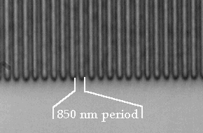
Fig. 2: Grating with a period of 850 nm exposed into a 250 nm thick photoresist layer on a GaAs-wafer
Rectangular gratings of 850 nm period with varying groove depths (55 nm to 180 nm) and different bar to space ratios had to be fabricated in order to find the optimal parameters for the excitation and light emission of surface plasmons. Due to the possible small feature size, the PR has been used to expose directly these required grating structures on the GaAs-LED-wafers. By changing the exposure time the width of the grating grooves has been systematically varied to find the optimum value for maximum surface-mode-emission from LEDs. Figure 2 shows a grating with a period of 850 nm exposed into a 250 nm thick photoresist layer on a GaAs-wafer. These gratings have been transferred into the substrate by ion-milling.
The good quality of the exposed gratings allowed an optimization of the LEDs. The far field radiation pattern and the external quantum efficiency of the LEDs have been measured. For p-polarized light the maximal peak-intensity was obtained at 90 nm and 120 nm groove-depth and a 1:1 bar to space ratio. The intensity was about 4 times higher than that of an unstructured LED. The beam divergences of the LED's were 7° (90 nm) and 10° (120 nm).
MBE (molecular beam epitaxy) techniques allow the epitaxial growth of various compounds. Model materials for optoelectronics are epitaxial layers of III-V semiconductors, mainly GaAs and related compounds. The controlled growth of single crystalline layers on an atomic scale makes it possible to design new materials with optimized electrical and optical characteristics.
Epitaxial growth of AlxGa1-xAs on GaAs gives a band discontinuity in the conduction and valence band. Intentional doping influences the Fermi levels and increases the band offset at the interface. Electrons move from the n-doped AlxGa1-xAs into the non-doped GaAs and form a two dimensional electron gas (2DEG). The offset and the bending of the bands prohibit the recombination of the carriers with the ionized impurities in the AlxGa1-xAs. Impurity scattering is the most dominant scattering mechanism at low temperatures. In a 2DEG this scattering process is drastically reduced due to the separation of carriers and impurities ("remote impurities"). This leads to electron mobilities up to 107 cm2/Vs (4.2 K).
The modular GEN II solid source MBE machine is a system specially designed for high quality growth of III-V materials. Eight different sources can be used to grow AlAs, InAs, GaAs and any ternary compound (AlGaAs, InGaAs, AlGaAs) with different doping concentrations of Si. In situ RHEED measurements are used to monitor surface conditions and growth rate.
A molecular beam epitaxy system for the growth of GaAs/GaAlAs heterostructures was installed and made "epiready" in 1994. The first epitaxial GaAs layers were grown in October 94 after baking and outgassing procedures of the system and the effusion cells. The first GaAs/AlGaAs layers with a 2DEG having mobilities exceeding 106 cm2/Vs (at 4 K, without illumination) could be realized within one year. Since May 1995, heterostructures with international quality can be produced on a regular basis.
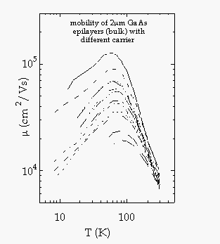
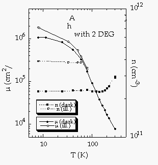
Fig. 3: Properties of the MBE grown epilayers.
Two dimensional electron gases (GaAs/AlGaAs heterostructures) were grown with mobilities up to 1.5·106 cm2/Vs at 4 K and 2.5·106 cm2/Vs after exposure to red light. The sheet carrier concentrations vary from 0.5 to 5·1011 /cm2. Characterization was done via temperature dependent hall measurements (4 K to 300 K), SdH measurements, and cyclotron resonance absorption. Additional confinement by structuring and etching leads to quantum wire and quantum dot regimes. The optical and transport behavior of these low dimensional systems is investigated (for a more detailed description please see section "Nano- and microelectronics").
Quantum wells were designed to have subband transition energies in the FIR regime below the optical phonon energies (36 meV). Sheet carrier concentrations from 1 to 4·1011/cm2 were realized by remote delta doping to have reasonable mobilities (reduced scattering) in the wells. Well thickness, growth temperatures, spacer thickness between wells and doped layers, and doping concentration were systematically varied from growth to growth. Carrier concentrations were determined from hall and SdH measurements, subband transition energies from transmission studies in an FFT spectrometer. Relaxation times of intersubband energies were measured with a free electron laser (FELIX, Amsterdam). For growth rate and well thickness analysis, a photoluminescence setup was installed (for a more detailed description please see sections "Far-Infrared-Spectroscopy" and "Optoelectronics").
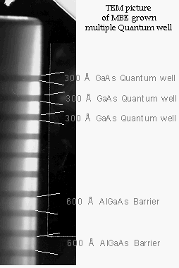
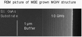
Fig. 4: TEM (left) and REM (right) pictures of MBE-grown Multiple Quantum Wells.
Multi Quantum Well structures (MQW) are grown on a diffusion stop layer (superlattice, not shown) and an 1 µm thick buffer layer to prevent diffusion of impurities from the bulk into the epilayers.
Carriers in the wells are set to 2·1011cm-2 by doping profiles in the AlGaAs barriers 300 Å remote from the wells (Si delta doping).
Resonant tunneling diodes (RTDs) with GaAs quantum wells and AlGaAs barriers were prepared. After characterization and optimization of these diodes, samples including stop layers (some monolayers consisting of pure AlAs) were fabricated. The first working "three terminal devices" with electron injectors, drift regions and a "filter" to separate ballistic from thermal carriers were realized in December 1995. Parallel to these activities, superlattice structures (GaAs/AlGaAs-superlattices with periods from 2 to 20 monolayers) were grown to investigate the doping behavior. Aim of this work is the realization of terahertz detectors and emitters (for a more detailed description please see section "Far-Infrared-Spectroscopy").
In this summary a short description of all those running projects of the institute of solid state electronics (fke) is given that are not directly involved in the growth of semiconductor materials but rely on III-V based samples and/or use devices patterned in the cleanroom (by optical, laser- or electron-beam lithography).
For vertical transport, tunneling spectroscopy is used to investigate nanostructured systems. Using a special double 2D GaAs-AlGaAs heterostructure, a situation can be achieved where electrons tunnel between a 2D electron system and quantum wires or quantum dots. By applying a voltage to the sample, the quantized states are shifted energetically with respect to each other, and therefore transitions between states of different dimensionality can be investigated. In terms of a transfer Hamiltonian formalism, the tunneling characteristics turn out to be the Fourier transforms of the wave functions in the 1D (0D) states, and therefore the experiments can be regarded as "Fourier transform tunneling spectroscopy".
Lateral transport experiments have been performed on systems consisting of few quantum wires. The lateral patterning of the sample surfaces has been achieved by electron beam lithography and laser holography. The electronic transport properties of these quasi-one-dimensional electronic systems were investigated at low temperatures using magnetic depopulation experiments. At higher temperatures, magnetophonon resonances (MPR) were investigated systematically for the first time. It has been shown that both methods yield the same results for 1D subband spacing, and that MPR are particularly useful for the investigation of samples with high quantization energies and a small number of occupied subbands. In the quantum limit, this is the only way to determine the subband spacing, since magnetic depopulation experiments do not work in this case.
Low temperature scanning tunneling microscopy (STM) studies were performed on quantum wires fabricated on GaAs-AlGaAs by laser holography and wet chemical etching. It was found that both tip and surface preparation have dramatic influence on the obtained results. Current-voltage curves were measured on the quantum wires and also in the depleted areas between the wires. On the wires, a tunneling current is observed for positive and negative sample bias, whereas in the depleted areas, tunneling is only observed for electron transitions from the valence band of the semiconductor into the STM tip. These features are due to surface depletion effects in the depleted areas. By comparison of current imaging spectroscopy data taken at room temperature and at T = 4.2 K, the width of the edge depletion can be determined directly.
The hot-carrier reliability of fully overlapped-LDD CMOS devices called FOND (Fully Overlapped Nitride-etch Defined device) is investigated. Significant improvement in the hot-carrier resistance of FOND technology compared to standard LDD devices with the same effective channel length is completely explained by modeling and various experiments. The results provide understanding of the experimentally obtained reliability behavior of 0.35 µm MOSFETs and can be applied to optimize the design rules for these devices.
The applicability of charge-pumping technique to characterize the oxide/silicon interface in standard power VDMOSFETs (Vertical Double-diffused MOSFETs) is studied. Qualitative analysis and analytical and numerical modeling show that charge-pumping measurements can be carried out in the subthreshold region. This conclusion is confirmed by various experimental results.
Within a cooperation between the Institute and Siemens Munich, an optical measurement system has been developed that allows the contactless detection of free carrier concentrations and of the local lattice temperature in integrated semiconductor devices from the backside of the chip. With that new measurement set-up (heterodyne interferometer), switching operation in single bipolar transistors and MOSFETs, as well as in complex integrated circuits, has been analyzed. Self-consistent modeling of the probed device has been carried out. Studies of laser-probe signals in MOSFETs (in depletion conditions) show the applicability of the optical system for the determination of the substrate doping level.
Our current activities are focused on the study of heating phenomena in power VDMOSFETs, where the local temperature of the silicon substrate is optically determined by laser-probe measurements. The experiments are supported by numerical modeling of the heat propagation and by conventional measurement techniques (pulsed I-V). In addition, we apply a homodyne interferometer for the experiments on power MOSFETs in order to enhance the detection sensitivity. Results of this analysis are the basis for studies of heating phenomena in SOI-MOS structures and MOSFETs on SIMOX-wafers.
At the end of 1995, a project has been started part of which considers the applicability of the backside-laserprober to the analysis of microwave signals (up to 20 GHz) in sub-micron devices.
Conventional AlGaAs/GaAs-DH LED's have a non-directional emission and a low external quantum efficiency. If, however, the surface of an LED is periodically structured and coated with a thin metal film, photons, which usually would be lost by total reflection, are coupled to surface plasmon (SP) at the metal-air interface. These SP decay by emitting p-polarized light.
In this work, rectangular gratings of 850 nm period with varying groove depths (55 nm to 180 nm) and various bar to space ratios were etched in order to find the optimal parameters for the excitation and light emission of surface plasmons. A 30 nm gold film was deposited on the grating.
The far field radiation pattern and the external quantum efficiency of the LEDs have been measured.. The beam divergences of the LEDs were 7° (90 nm) and 10° (120 nm). Broadening and a splitting of the peaks with increasing groove depths has been observed. This is due to a shift of the SP dispersion relation to higher k-values. An increase of the external quantum efficiency has also been observed, but this increase is mainly caused by the reduced light absorption in the GaAs top-layer.
Structuring of vertical cavity surface emitting semiconductor laser diodes (VCSEL) based on GaAs/AlGaAs-structures with vertical and lateral dimensions in the order of magnitude of a few microns can only be achieved successfully by etching-techniques with anisotropic characteristics and little material selectivity. Ion milling complies with both demands to a high degree: It could be shown that etching of cavities based on VCSEL structures with vertical dimensions up to 3.5 microns with steep flanks (70 degrees) by using standard-techniques for the production of etch-masks (optical lithography) is possible. A numerical simulation was developed to calculate the development of the surface of the sample under ion-bombardment.
Furthermore it was shown that the monolithic integration of VCSEL and photodetectors is possible: An integrated LED-detector device was developed by using the vertical VCSEL structure both as LED and detector.
Whether a semiconductor can be used for laser operation or not is determined by a population inversion of charge carriers, which is governed by the lifetime of electrons in excited states. In this work, the lifetime of electrons in excited states is investigated. The intersubband lifetime in GaAs/AlGaAs quantum well samples was directly measured. These pump and probe experiments were performed using the free electron laser "FELIX" in Nieuwegein (the Netherlands). The measured lifetimes of 400 ps in GaAs/AlGaAs are compared to calculated results of a theoretical model. This comparison shows that a combination of electron-electron scattering and optical and acoustical phonon scattering is limiting the electronic lifetime.
Up to now there is a large number of semiconductor lasers delivering coherent radiation in the spectral range of the visible and the near infrared. In the spectral range of the far infrared (30 µm < < 1000 µm) there are only two types of semiconductor lasers. These are the p-Ge cyclotron resonance laser and the p-Ge intervalenceband laser. Both laser types are tunable over a large frequency range. In this work, p-Ge lasers with various crystallographic orientations, sizes, and impurity concentrations are produced and investigated. It was shown in detail that the spectrum of the intervalenceband laser does depend sensitively on the acceptor species.
In this work, various methods for characterizing low dimensional electron systems on GaAs/AlGaAs heterostructures are presented and discussed. The main focus is on magnetotransport measurements and the spectroscopy in the far infrared. Starting from non-structured two dimensional systems, the impact of lateral potential modulations on the electronic properties is investigated. Using holographic lithography and wet chemical etching, weakly and strongly modulated one- and zero-dimensional systems as well as isolated quantum wires are prepared. In these low dimensional systems, one expects to find collective charge density and single particle excitations.
In modulated 1D systems, the magnetoresistance shows a negative differential behavior and the appearance of a prominent maximum in the low magnetic field region, which can be explained in terms of the commensurability of the cyclotron radius and the lateral period of the wire pattern. The optically detected excitations in the far infrared reveal the occurrence of magnetoplasmons due to the quantization of the electronic states in the wires. From the frequency of this localized plasmons the subband quantization and the electrical width of the quantum wires are derived. Applying the above bandgap illumination to the wet chemical etched samples, a change from an isolated quantum wire via a modulated 1D system to a pure two-dimensional system could be achieved.
In the project Po8179-MAT, ceramic high temperature superconductors (HTc) were composed, and out of these polycrystalline samples single crystalline films were prepared that were investigated in transport and optical measurements. The technology for preparing, doping, and structuring was developed, and the impact of the carrier concentration on the superconducting properties of the HTc-films was analyzed. In this project, thin YBCO-films with grating structures of the width 5 µm were defined. Experimental data and theoretical analysis show that these films could be used as a bolometer for the IR and may be suited for imaging systems at 77 K.
The improvements in the perfection of growth of semiconductor heterostructures (e.g. superlattices) using molecular beam epitaxy (MBE) have revived interest in making an extremely fast emitter of electromagnetic radiation. One of the basic requirements to realize the so-called Bloch oscillator is a long enough mean free path (mfp) of the oscillating hot electrons.
In order to investigate the mfp of ballistic hot electrons, a three terminal device was designed. In such devices, hot electrons are injected into a thin (10 nm) highly doped GaAs base via an AlGaAs tunnel barrier and are collected at the collector. As the hot electrons traverse the superlattice that has been grown in between the base and collector layer, they are used to probe scattering events.
Institut für Festkörperelektronik, TU Wien, Floragasse 7, 1040 Wien
Last Name      First Name     Status              Remarks

Auer           Peter          student

Eder           Claudia        graduate student

Finger         Norman         student

Freisleben     Stefan         student

Gmachl         Claire         Assistant Prof.

Golshani       Alireza        graduate student

Gornik         Erich          Full Prof.

Habas          Predrag        Post Doc            100 % GMe

Hainberger     Rainer         student

Hauser         Markus         Post Doc            75% GMe funding

Heiß           Wolfgang       graduate student

Hvozdara       Lubos          student

Köck           Anton          Assistant Prof.

Kröll          Peter          technician

Lakatha        Harald         graduate student

Langmann       Gottfried      technician

Liu            Jian           student

Ploner         Guido          graduate student

Pogany         Dionyz         Post Doc            100 % GMe

Prinzinger     Johannes       technician

Rauch          Christoph      graduate student

Roßkopf        Valentin       graduate student    75% GMe funding

Seliger        Norbert        graduate student    100% GMe

Smoliner       Jürgen         Assistant Prof.

Straßer        Gottfried      Assistant Prof.

Unterrainer    Karl           Assistant Prof.

Zobl           Reinhard       student

Zotl           Ernst          student