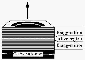
Fig. 1: The geometry of a VCSEL-structure with a Bragg-mirror both on the substrate-side and on top. The Bragg-mirror consists of 20 - 30 pairs of alternating (l/4)-layers of GaAs/Al(Ga)As.
Two-dimensional arrays of vertical-cavity-surface-emitting laser diodes (VCSELs) have been fabricated by an ion-milling etching-technique. The etching of large-area VCSEL-arrays has been successfully demonstrated. A 2 x 2 array of VCSELs has been fully processed and characterized. The results achieved from these VCSELs clearly demonstrate that ion-milling is a very useful technique for the etching of VCSELs.
Vertical surface emitting laser diodes (VCSELs) are an excellent answer to the need of surface-emitting lasers due to their small size, planar geometry, integrability and potentials for high power and high quality beams. VCSELs can be fabricated in two-dimensional arrays, because they have integrated resonator mirrors (Bragg-mirrors) and require no cleavage. Therefore VCSELs are ideal candidates as light emitters in integrated optoelectronics devices.
The goal of this project was the fabrication of two-dimensional arrays of VCSELs through application of a proper etching technique. The complex processing of VCSELs requires more sophisticated etching techniques than the simple wet-chemical etching technique. Therefore, an Ion-milling etching technique was used for the fabrication of two-dimensional VCSEL-arrays.
VCSELs are grown by molecular-beam-epitaxy (MBE) or by metal-organic-chemical-vapor deposition (MOCVD). The geometry of a VCSEL-structure is shown in Fig. 1. First a Bragg-mirror, which consists of 20 - 30 pairs of alternating (l/4) GaAs/ Al(Ga)As layers, is grown on the substrate. The thickness of a (l/4) layer is typically between 60 nm and 80 nm. Next is a cladding layer of AlGaAs, the GaAs active region and a further cladding layer of AlGaAs. The structure is completed by a second Bragg-mirror on top, which consists of another 20 - 30 pairs alternating (l/4) GaAs/AlGaAs layers. The total thickness of the entire grown structure is 3 - 5 µm.
Fig. 1: The geometry of a VCSEL-structure with a Bragg-mirror both on the substrate-side and on top. The Bragg-mirror consists of 20 - 30 pairs of alternating (l/4)-layers of GaAs/Al(Ga)As.
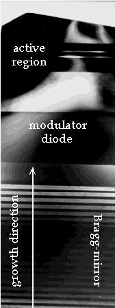
Fig. 2: TEM photograph of a frequency tunable VCSEL.
In addition to conventional VCSELs with Bragg-mirrors on the substrate side and on the top side, frequency tunable VCSELs with integrated modulators have been processed. This type of VCSEL is of high importance for wavelength-division-multiplexing techniques in optical communication. These special VCSELs have an integrated modulator diode in the cavity, but no Bragg-mirror on top. To illustrate the real geometry of a VCSEL-structure, a TEM photograph of a frequency tunable VCSEL is shown in Fig. 2. This sample consists of a p-n-p structure embedded between an undoped Bragg mirror with 24 pairs of alternating layers of AlAs and Al0.10Ga0.90As at the bottom and a 500 Å thick silver mirror on top. The modulator diode is formed by an Al0.15Ga0.85As pn-junction with an intermediate AlxGa1xAs (x = 30/15) grading layer. The modulator is directly followed by a GaAs/AlGaAs double-hetero junction laser diode. The two diodes share the same n-contact layer, which is directly connected to ground during experiments thus electrically separating the two diodes.
For processing VCSELs, single mesas have to be etched into the substrate. This requires at least one etching step where the whole structure is etched down to the substrate. The etching of the alternating GaAs/Al(Ga)As mirror-layers cannot be achieved by conventional wet-chemical etching techniques, because the different etching-rates of the GaAs- and the Al(Ga)As layers result in highly non-uniform etching walls. This limits the minimum size-feature, which can be etched and strongly limits the electronic and optical characteristics of the VCSEL. In addition, wet chemical etching is not suitable due to very strong underetching in the upper Bragg mirror.
Therefore, the processing of VCSELs requires a more sophisticated etching technique, which is less material selective than the wet-chemical etching technique. An ion-milling machine (Millatron 8) using Ar+-Ions with energies between 200 eV and 1000 eV was used to develop the etching technique for processing the VCSEL structure into mesas.
First of all, the etching rates of proper etching-masks have been measured. Photoresist was found to be a useful mask for the etching process. The etching rate of photoresist is around 4 nm/min. Also Ti-films and Cr-films were used as etching masks. The etching rates of both metals, however, are approximately the same as in case of the photoresist. As the evaporation of the metal-masks requires an additional processing step, photoresist is more suitable.
The etching rates of GaAs and AlGaAs are 17 - 19 nm/min and 15 - 18 nm/min, respectively, depending on the angle of incidence of the sputtering Ar+-Ions. As the difference between both rates is small, this technique is very well suited for the etching of the Bragg-mirrors. An Ion-milling simulation program has been developed to predict etching profiles and has been found to be in excellent agreement with the experimental results [1], [2].
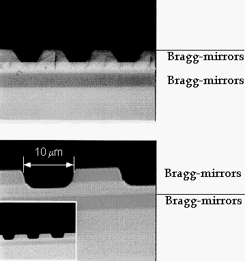
Fig. 3: Arrays of VCSEL-structures etched by ion-milling.
Fig. 3 shows the result of etched two-dimensional VCSEL-arrays with Bragg-mirrors on the top and on the substrate side. While in GaAs-substrates even vertical walls have been achieved by ion-milling, Bragg-mirrors of VCSELs show a steepness between 60o and 80o. This, however, can still be optimized to achieve vertical walls.
After the setup of the ion-milling etching technique and the demonstration of etched two-dimensional VCSEL-arrays, a 2 x 2 array of VCSELs was fully processed and electrically contacted to measure the performance of ion-milled VCSELs. For these arrays, VCSELs with integrated modulator-diodes have been used. First the laser diode is mesa etched (30 x 30 µm) to the common n-contact layer. Further etching defines a rectangular mesa for the modulator diode. Subsequent evaporation of the top, intermediate, and bottom contacts gives independent access to the laser and the modulator diode. The top contact shows a window with a silver coating where the laser emission is coupled out.
All measurements were carried out at room temperature under pulsed current operation. Fig. 4 shows the characteristic PIV diagram of a typical VCSEL. Its threshold current density varies from 3 kA/cm2 to 9 kA/cm2, which is a very reasonable value for this structure. Fig. 5 shows an emission spectrum of the laser diode, which demonstrates the influence of lateral variations of the injected current on their transversal mode spectra. For high modulator current (higher than 50 mA) the VCSELs showed a transversal mode switching from TEM00 to TEM10 as a result of a laterally inhomogeneous modulation of the cavity. (The order of the modes has been identified by means of spectral evaluation and their near field patterns.) The wavelength tuning of these VCSELs and the effect of the modulator current is discussed in detail in [3] - [8].
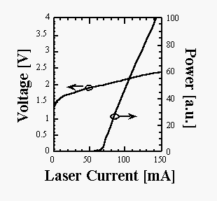
Fig. 4: P-I-V diagram of a GaAs/AlGaAs double-hetero junction VCSEL with an integrated AlGaAs pn-modulator diode.
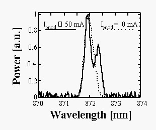
Fig. 5: Emission spectra of a longitudinally single-mode VCSEL showing transversal mode switching with the modulator current.
Within this project, two-dimensional arrays of VCSELs have been fabricated by an ion-milling etching-technique, which has been set up. The etching of large-area VCSEL arrays has been successfully demonstrated. A 2 x 2 array of VCSELs has been fully processed and characterized. The results achieved from these VCSELs clearly demonstrate that ion-milling is a very useful technique for the etching of VCSELs. It will be used for the fabrication of larger VCSEL arrays as a source for direct optical interconnects between stacked boards in computers.
This work was partly supported by the "Stiftung Volkswagenwerk", Hannover, Germany.
[1] N. Finger, R. Hainberger, C. Gmachl, A. Köck, E. Gornik, J. F. Walker: "Herstellung von zweidimensionalen Feldern oberflächenemittierender Halbleiter-Laserdioden mit vertikalem Resonator mittels Ion-Milling", 45. Jahrestagung der Österreichischen Physikalischen Gesellschaft, 18.-22. September 1995, Leoben, Austria.
[2] A. Köck: "Präparation und Charakterisierung von frequenzdurchstimmbaren VCSEL", Photonik-Symposium, der Volkswagen-Stiftung, 4. - 6. Oktober 1995, Braunschweig, Germany.
[3] C. Gmachl, A. Köck, A. Golshani, S. Freisleben, E. Gornik, J.F. Walker: "Emissionscharakteristik von frequenzverstimmbaren oberflächenemittierenden GaAs/AlGaAs-Halbleiterlaserdioden mit vertikalem Resonator", Frühjahrstagung der Deutschen Physikalischen Gesellschaft, Fachverband Quantenoptik, 27. Februar - 3. März 1995, Innsbruck, Austria.
[4] C. Gmachl, A. Golshani, N. Finger, A. Köck, E. Gornik: "Preparation and characterization of vertical-cavity surface-emitting lasers with integrated modulators", 7th Brazilian Workshop on Semiconductor Physics, 16. - 17. Juli 1995, Rio de Janeiro, Brasil.
[5] C. Gmachl, A. Golshani, A. Köck, E. Gornik; J.F. Walker: "Vertical-cavity surface-emitting lasers with monolithically integrated modulators", NATO-Workshop "Quantum Optics in Wavelength Scale Structures", 26. August - 2. September 1995, Cargese, Corsica, France.
[6] C. Gmachl, A. Golshani, A. Köck, E. Gornik; J.F. Walker: "Vertical-cavity surface-emitting lasers with monolithically integrated modulators", Proceedings of the NATO-Workshop "Quantum Optics in Wavelength Scale Structures", 26. August - 2. September 1995, Cargese, Corsica, France, to be published in NATO Series, Kluwer Academic.
[7] C. Gmachl, A. Golshani, A. Köck, E. Gornik; J.F. Walker: "Frequency tuning of VCSELs by a monolithically integrated modulator diode", 8th Annual Meeting IEEE Lasers and Electro-Optics Society, 30. October - 2. November 1995, San Francisco, CA, USA.
[8] C. Gmachl: "Frequency tuning of VCSELs by a monolithically integrated modulator diode", Oral presentation at AT&T Bell Laboratories, Murray Hill, NJ, USA 1995.
Institut für Festkörperelektronik, TU Wien, Floragasse 7, 1040 Wien
Last Name      First Name     Status              Remarks

Finger         Norman         undergraduate
                              student

Gmachl         Claire         graduate student

Hainberger     Rainer         undergraduate
                              student

Köck           Anton          assistant
                              professor

Gornik         Erich          full professor

Walker         John F.        associate
                              professor