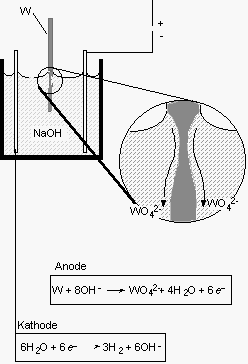
Fig. 1: Experimental setup for electrochemical tip fabrication.
Institut für Festkörperelektronik, Technische Universität
Wien,
Floragasse 7, A-1040 Vienna, Austria
In this project, Scanning Tunneling Spectroscopy (STM) studies on (100) surfaces of GaAs/AlGaAs quantum wire structures in dry nitrogen ambient are reported. For this purpose, ultrafine tungsten tips were fabricated by electrochemical etching. Measuring the IV-curves on the wires and in the etched areas between the wires, distinct local differences between I-V are found even at room temperatures. This enables us to clearly observe quantum wire regions with current imaging tunneling spectroscopy at 300K. The observed differences are ascribed to the internal potential profile in the sub surface regions of the sample. In this sense, the STM tip can be understood as a potential probe of the sub surface regions of a laterally structured sample.
The goal of the project was to use a scanning tunneling microscope (STM) on nanostructures that were fabricated by laser holography on GaAs-AlGaAs heterostructures. As the scanning range of the STM is limited to a range of 10 µm x 10 µm, large arrays of quantum wires having a period of typically 0.5 µm were fabricated on the samples. Thus, several quantum wires are always within the scanning range of the STM.
On such a large array of laserholographic quantum wires or quantum dots a STM can be used to establish a contact to individual structures inside the array. The STM at the Institut für Festkörperelektronik is capable to work at low temperatures and at high magnetic fields allowing magnetotunneling experiments on single quantum structures. Thus, low temperature images of the samples can be recorded and due to the atomic resolution, even local tunneling characteristics can be measured on single structures.
To perform successful measurements on nanostructured systems like quantum wires and quantum dots, one has to make sure that the radius of the used tip is small compared to the size of the investigated structures. Especially the large aspect ratio of the surface profile (stepsize 10 nm) requires ultrafine STM tips for proper surface scans. To minimize the influence of the STM tip geometry on the results, special electrochemically etched tips were used. A wire acts as an electrode in an electrochemical cell and is etched by an external voltage. Figure 1 schematically shows the corresponding experimental setup. To produce ultrafine tips, a process was realized that is sensitive to strong changes in the cell current and stops the etching process when the part of the wire that is below the surface of the etchant falls off. For this purpose, a tungsten wire (0.5 mm diameter) is dipped 1 mm into a 1 mol NaOH etchant.
Fig. 1: Experimental setup for electrochemical tip fabrication.
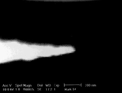
Fig. 2: Scanning electron microscope image of a typical tip. The tip radius is smaller than 50 nm.
The initial voltage is in the range between +6V and +20V. Changes in the cell resistance are electronically derived and compared with a reference value Vth. This value is chosen in a way that a comparator triggers at that moment when the lower part of the wire falls off. The trigger signal switches the external voltage off and stops further etching, which would result in a destruction of the tip. In this way, tips with radii below 50 nm and arbitrary aspect ratio can be realized (see Fig. 2).
One of the most difficult things for successful STM measurements was the choice of STM suitable samples on the basis of GaAs-AlGaAs heterostructures. In STM measurements on conventional samples, electrons have to tunnel through the vacuum barrier, then through an GaAs cap layer, and finally through a thick AlGaAs barrier, before they can reach the collector electrode. The resulting transmission coefficients of all barriers together result in extremely small tunneling currents, which cannot be measured with the present electronics of our STM. To overcome these problems, inverted heterostructures were used. On such samples, the 2DEG is located on top of the AlGaAs directly below the surface. If the surface doping is high enough, the barrier to the surface is thin and the resistance between the 2D channel and the surface can be neglected. Now tunneling processes between tip and 2D gas can be investigated directly.
In the following, we report on first STM studies of wet chemically etched quantum wire structures on inverted heterostructure samples in a dry nitrogen ambient at room temperature. Even at 300 K we find a distinct spectroscopic difference between non etched sample regions and regions where the underlying electron gas has been depleted by etching. This difference enables us to detect the quantum wire regions from CITS and not only from topographic imaging.
The samples which we used for the experiments were inverted GaAs/AlGaAs heterostructures that consist of a semi-insulating substrate, a 2 µm GaAs buffer layer, followed by a 200 Å undoped AlxGa1-xAs layer, a 50Å doped AlxGa1-xAs (ND = 2x1018 cm3) layer and again by a 250Å undoped AlxGa1-xAs spacer layer (x = 0.35). On top, the samples consist of 800Å of low doped GaAs (ND = 1.2x1015 cm-3) and finally of a 150 Å highly doped GaAs surface layer (ND = 6.2x1018 cm-3). The structure results in a concentration of free electrons close to both the GaAs/AlGaAs interface and the AlGaAs/GaAs interface even at 300K.
Lateral pattering of the sample was achieved by laser holography and subsequent wet chemical etching, which partially depleted the underlying upper electron layer of free carriers. The electron layer underneath the AlGaAs barrier is not affected by this treatment. This procedure yielded large arrays of quantum wires with a period of 475 nm with an etch depth of about 120Å. Note that despite this fine etching the uppermost layer of the sample does not have an altered dopant concentration, as some 30 Å of the highly doped surface layer are still left. At least two ohmic contacts were prepared by standard Au-Au/Ge-Ni alloying. The STM tip is then used to probe the sample by measuring the tunneling current between tip and sample as a function of applied voltage and/or position (Fig. 3).
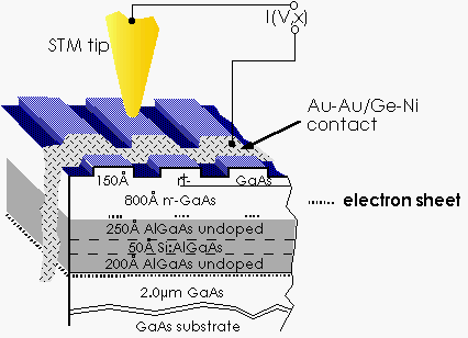
Fig. 3: Sample structure used for the measurements. Carriers are concentrated close to both the GaAs/AlGaAs and the AlGaAs/GaAs interfaces. After etching, some regions of the upper electron layer are depleted of free carriers.
A key element for the experiments was surface preparation, as all measurements were carried out in ambient pressure. In order to remove native oxides, the samples were dipped into a HCl:H2O solution for 30 sec, shortly rinsed in DI water and blown dry with nitrogen. Afterwards they were immediately transferred into the STM chamber, which was purged with dry N2 to prevent further oxidation of the surface. After this treatment, only a thin oxide layer remains, resulting in exact topographic profiles of the etched structures. The dry N2 flow was continued during the measurements as otherwise the STM image deteriorated within minutes. A comparable effect was found by Pischow et al. [1]. They state that the water bound to the native oxide layer of polished Si wafers, not so much the oxide layer itself, causes difficulties associated with STM work. We conclude that the N2 flow prevents condensation of water at the surface and allows satisfying tunneling conditions despite a possible thin oxide layer.
Special attention was also paid to tip geometry. For sample structures with large corrugations in comparison to atomic dimensions, artifacts are readily introduced into topographic images due to the influence of tip shape. To prevent this, only sharp Au-sputtered W-tips with radii of less than 20 nm have been used. The aim of this work was to identify quantum wire regions on (100) surfaces from spectroscopic studies, not only from topographic imaging. This is not straightforward, since at the etched regions the sample is depleted of free carriers. This could lead to charging effects that prevent STM studies. Fig. 4 (a) shows I-V curves obtained at 300K on non-etched - i.e. on the wire - and on etched regions of the sample. A distinct qualitative spectroscopic difference between the etched and the non-etched regions is found. In the non-etched regions I-V curves resemble curves expected for a metal-vacuum-metal (highly doped semiconductor) junction in the intermediate emission regime between vacuum tunneling and the Fowler-Nordheim region [2]. We obtained equivalent curves on unstructured reference samples. In the etched regions, however, the I-V curves show a diode-like behavior with no current flow for positive sample bias. As mentioned above, in this case one might even expect current flow to be prohibited for both bias directions, as charging of the sample in the depleted areas might be expected immediately due to the lack of free carriers. This was not observed. Rather, standard topographic imaging and tunnel gap control are still possible for all sample regions if the sample bias Vt is chosen to be negative.
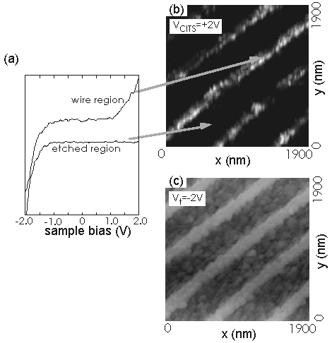
Fig. 4: I-V curves obtained on non-etched (i.e. wire) and etched areas of the quantum wire sample with L = 475 nm (a). For the etched regions, injection of electrons into the sample is not possible. Current flow (bright lines) in the CITS image measured at VCITS = +2 V thus corresponds to the quantum wire regions (b). Quantum wires in the simultaneously obtained topographic image (c). Tunneling parameters for the gap hold were set to -2 V/-100 pA in all cases.
The measured spectroscopic features can be utilized for CITS. For CITS, the sample surface is scanned in standard constant current mode with suitable parameters for the tunnel gap hold. Additionally, the feedback control loop is opened for specified pixels. The voltage is then set to some chosen value and the resulting current is measured without feedback control. The current image thus represents the current value for a given voltage as a function of the lateral x and y coordinates. CITS can have the same resolution as the topographic image.
Fig. 4 (b) shows the 1.9 µm x 1.9 µm CITS image, Fig. 4 (c) the simultaneously obtained topographic image of a quantum wire array with a period of L = 475 nm. For fixing the tunnel gap and for topographic imaging, a negative sample bias was chosen. The CITS image was measured at positive sample bias. As expected, no current can be detected in between the wires (dark region). The quantum wire regions, however, are clearly visible in the CITS image (bright).
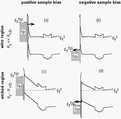
Fig. 5: Sample band profiles and tip Fermi level position for the wire region at positive (a) and negative sample bias (b) as well as for the etched sample region at positive (c) and negative sample bias (d). The arrows indicate current flow across the vacuum barrier. At the etched region, current flow is prohibited for positive sample bias due to the large voltage drop in the sample.
Figure 5 explains the observed spectroscopic differences by taking into account self consistently calculated semiconductor band profiles and tip Fermi level positions. Figure 5 (a) shows the situation for non etched regions of the sample. Due to the special structure of our samples (very small surface space charge region due to high doping), the resistance Rs from the upper electron layer to the sample surface is very low compared to the tunneling resistance Rvb across the vacuum barrier. This could be confirmed in previous measurements [3]. An electron injected from the STM into the sample will thus be collected in the upper electron layer. The collection will take place by surface states and subsequent tunneling through the surface space charge layer or by direct injection into the semiconductor conduction band. For negative sample bias (Fig. 5 (b)), mainly electrons from the valence band of the semiconductor will tunnel through the vacuum barrier. Recombination of holes with free electrons from the sub surface electron layer via surface states will prevent charging of the sample.
In the etched regions of the sample where the upper electron layer is depleted, Rs is much larger due to the enhanced depletion region at the sample surface. Thus a part of the applied voltage will also drop across the sample, not only across the vacuum barrier. Additionally, there exists an n--n+-junction between the etched and the non-etched regions, where free carriers are present. This leads to an internal diode Rd.
Figure 5 (c) shows the situation for positive sample bias. Due to the large voltage drop in the sample the tip Fermi level can not be raised above the Schottky barrier at the sample surface. This rules out carrier injection into the conduction band. However, for negative sample bias, electrons are injected into the etched region from the wire regions by forward biasing the internal n+-n--diode. These will be able to reach the sample surface as the tunneling voltage this time reduces Rs. Thus current flow without charging of the sample is possible despite the fact that this region of the sample is depleted of free carriers. As mentioned above, this is very important as it allows standard topographic imaging of our samples at Vt < 0.
In summary, it was shown that an STM can be used to characterize sub surface quantum wire arrays at 300K and in ambient pressure. By local injection of carriers into a special sample structure, the spectroscopic differences between etched and non-etched regions can be utilized for CITS. The observed differences are ascribed to the internal potential profile in the sub surface regions of the sample. In this sense, the STM tip can be understood as a potential probe of the sub surface regions of a laterally structured sample.
[1] K.A. Pischow and J.M. Molarius, Nanotechnology 5, 80 (1994).
[2] C.J. Chen: Introduction to Scanning Tunneling Microscopy, Oxford University Press, New York, Oxford 1993.
[3] W. Demmerle, J. Smoliner, G. Berthold, E. Gornik, G. Wiemann und W. Schlapp, Phys. Rev. B 44, 3090 (1991).
Institut für Festkörperelektronik, TU Wien, Floragasse 7, 1040 Wien
Last Name      First Name     Status              Remarks

Eder           Claudia        PhD Student

Hauser         Markus         research scientist

Roßkopf        Valentin       PhD Student