Installation and Operation of the Electron Beam Lithography System
G. Straßer, M. Hauser, G. Ploner, E. Zotl, A. Köck,
A. Golshani, E. Gornik
Institut für Festkörperelektronik, Technische Universität
Wien,
Floragasse 7, A-1040 Vienna, Austria
The existing electron beam lithography (EBL) system consisting
of a slightly modified JEOL 6400F with beam steering soft- and
hardware was enhanced by an additional lithography control system.
The combined EBL system yields higher resolution and is capable
of marker recognition, correction of field distortion, size and
rotational corrections implemented in fast hardware. It was used
to realize nanostructured resist masks on GaAs substrates produced
by G. Straßer, Prof. M. Heiblum (Weizmann Institute of Science,
Israel) and Dr. J. Walker (Laboratorio TASC, Italy). These masks
were wet chemically etched to form semiconductor quantum wire
arrays and single quantum wires. Investigations of lateral transport
of the wire arrays revealed new correlation effects. On single
wires high field transport was investigated. The EBL system was
also used as a tool for the optimization of vertical emitting
heterostructure lasers, which led to strongly enhanced far field
patterns.
Introduction
The EBL system at the Institute of Solid State Electronics was
used for miscellaneous applications, ranging from low temperature
lateral transport investigations of quantum wire arrays and single
quantum wires to air bridged high speed Schottky diodes for THz
devices and fs-correlation detectors operating at room temperature.
It was also found to be an essential analysis tool used in the
optimization process for surface gratings used in vertical emitting
laser diodes.
Electronic Properties of Low Dimensional Electron Systems
Magnetophonon resonances (MPR) have been clearly resolved on nanoscale
arrays of quasi one dimensional quantum wires and were used for
the first time to systematically study the characteristic properties
of such systems.
At temperatures around 100 K, MPR result from resonant scattering
of electrons by LO phonons between electronic sublevels induced
by the confining potential. The resulting resonant structures
were used to investigate subband spacings and the polaron mass
of electrons in these one dimensional systems. This is particularly
useful for quantum wires near the quantum limit when traditional
methods for the characterization of 1D systems fail due to the
low number of occupied subbands. By variation of the electron
density in the quantum wire systems a situation can be achieved
where a decreasing number of subbands are occupied. It was found
that the MPR is strongest in cases where the electron density
is too low for classical magnetic depopulation experiments to
yield reliable information. We found that the subband spacing
in these quantum wire systems increases steeply when the electron
density is decreased. Compared to the 2DES, the polaron mass in
1D systems is larger and increases with decreasing 1D electron
density, which is caused by stronger electron-LO phonon coupling
due to reduced screening.
In systems containing only a few (up to five) ballistic quantum
wires, which were prepared by electron beam lithography and wet
chemical etching (Fig. 1), additional structures in the magnetoresistance
at low magnetic fields could be observed (Fig. 2). Channel resistance
peaks with a superimposed fine structure develop at relatively
high current densities. They can be explained by the assumption
that electrons exiting one quantum wire into the 2DES are magnetically
focused into the adjacent wire after specular scattering at the
boundary of the etched region forming the spacing between the
1D wires (Fig. 3). This coherent focusing causes interference
effects which lead to fine structured peaks in the magnetoresistance.
In further experiments the dependence of this effect on temperature
and on the length of the quantum wires is investigated. It is
expected that the results of forthcoming measurements can be used
to determine the phase coherence lengths in quantum wires.
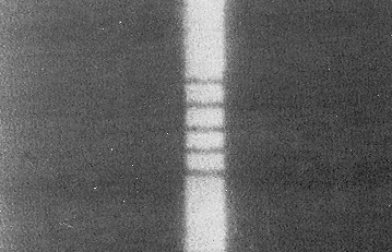
Fig. 1: Five wet chemically etched quantum wires (optical microscope,
magnification = 2500x). The quantum wires are 2 µm long.
The dark areas to the left and to the right are 2DEG used as 'contacts'
to the quantum wires. The annealed contacts to the 2DEG are not
shown.
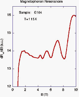
Fig. 2: Magnetophonon resonances at a temperature of 115 K in
an array of quantum wires.
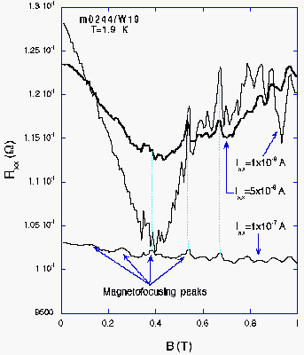
Fig. 3: Additional structures in the magnetoresistance of an array
of quantum wires for three different currents (magnetofocusing
peaks).
High Field Transport on Single Wires
Investigations of high field transport measurements on single
wires etched into the 2DEG of standard GaAs/AlGaAs heterostructures
a reduction of the channel resistance at high fields was found.
It can be attributed to the reduced dimension of the charge carriers
due to strongly reduced electron-electron scattering and a grossly
changed interaction of electrons and phonons in one dimension
[2].
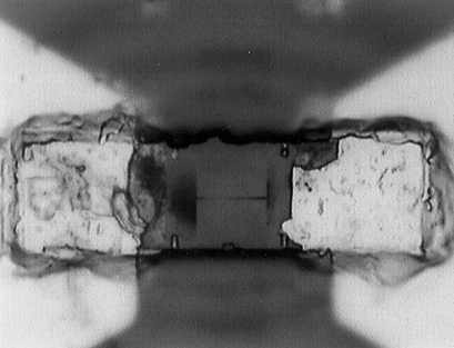
Fig. 4: Single quantum wire 20 µm long (optical microscope).
The mesa is 60 µm x 20 µm. The resist mask used to produce
the quantum wire by wet chemical etching is clearly distinguished,
since the electron beam resist is removed in a later processing
step.
Fast GaAs Schottky Diodes for THz Applications
Performance of GaAs based Schottky diodes for the THz regime is
strongly influenced by the capacity of the Schottky contact and
therefore its area. A reduction of the size of the contact pad
has been shown to result in very fast diodes suitable for THz
applications. A new method for the fabrication of such diodes
is being developed. It is based on an air bridged Schottky contact
with extremely small capacity. The size of the contact pad is
in the range of 100 nm x 100 nm or smaller. The stray capacity
of the leads is further reduced by air bridging.
A tri-level PMMA-based electron beam resist system is employed
to form one lead of the THz diode. By variation of the exposure
dose the lift off behavior of this system can be changed. Regions
with higher dose form contacts to the GaAs substrate, whereas
lower dose areas lead to bridges remote of the substrate. This
can clearly be seen in Fig. 5 showing part of an array of rather
large sized Au-air bridges on a GaAs substrate. This test pattern
was used during development of the EBL air bridge technology.
Further optimization of this process together with standard optical
lithography steps is necessary to develop fully functional THz
diodes.
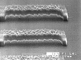
Fig. 5: Two air-bridges made of 100 nm thick gold (electron microscope).
It can clearly be seen that the gold, later to be used as Schottky
contact for THz diodes, clears the substrate at a distance of
about 2 µm. The bridge is about 250 nm high. The size of
the contact pads at the right hand side is about 100 nm x 1 µm.
For application in a high speed device, further optimization is
obviously needed.
Fabrication and Optimization of Surface Gratings for Vertical Emitting Laser Diodes
In semiconductor laser technology one is usually faced with the
fabrication of very small structures such as gratings with periods
varying from 200 - 750 nm used as couplers in DFB/DBR and SME
laser diodes.
Effective techniques to fabricate these small structures are laser
holography and EBL, since conventional optical lithography techniques
are limited in fabricating structures of such small sizes. Obviously,
standard optical microscopy can not be employed for the analysis
of such small sized structures. Therefore, EB microscopy was used
as a vital analysis tool (Figs. 6 and 7). Many repeated steps
of photolithography, ion milling and analysis by electron beam
microscopy led to optimized surface gratings [3, 4].
Laser Holography
Laser holography is based on the interference of two laser beams
used to expose standard photoresists. The period of the interference
pattern depends on the angle between the two incident beams and
the laser wavelength and is therefore limited to half of the laser
wavelength. In our setup, the angle between the sample and the
reflecting mirror is chosen to be 90°, and the distance between
the source and the sample holder assembly is very large compared
to the laser wavelength, so that the curvature of the interference
pattern is practically zero. The laser source is a He-Cd laser
operating at 325 nm with 28 mW of output power. The grating period
can be calculated as , where and are grating period and laser
wavelength and is the incident angle.
Photo Resists and Fabrication Process
Photo resists used to fabricate surface gratings must satisfy
the following conditions in order to fulfill the requirements
for successful grating fabrication:
- Capability of submicron resolution with high contrast;
- Suitability for broadband and monochromatic exposure;
- Good adhesion for etching;
- High thermal stability;
- Wide process latitude.
Unfortunately, standard photo resists are not optimized for requirements
such as stated above.
Positive Resist AZ 6615
In order to achieve a reasonable grating depth by wet chemical
etching the resist must reveal steep edges. Positive resist characteristics
make it possible to fabricate such structures. The optimized process
used for fabrication of 425 nm surface gratings is given in the
following:
- HCl dip; HCl dip serves to remove organic compounds from the
sample's surface in order to achieve a better adhesion to the
surface.
- Spin coating the sample with AZ 6615 resist for 35 s at 10000
rpm. This corresponds to a resist thickness of 1.2µm.
- Pre-exposure bake for 45 s at 100 °C.
- Exposure by laser for 45 s.
- Develop in AZ 726 MIF for 30 s and rinse thoroughly.
- Post-exposure bake for 60 s at 120 °C.
- O2-Plasma etching for 3 minutes with 100 W power. This removes
the rest of resist from the sample's surface and helps to achieve
a homogeneous etched surface.
- Wet chemical etching by a solution of AZ 726 MIF, H2O, H2O2
and tenside
The etching rate is about 20 nm/min and is fully reproducible.
To fabricate gratings with other periods and duty ratios one should
change the exposure duration and development time, i.e., longer
exposures decrease the bridge to trench ratio. For smaller grating
periods the exposure time should be increased to achieve a one
to one duty ratio. The developing time should be kept minimum
provided the exposed surface is completely developed. Figure 6
shows a grating of period 425 nm fabricated by positive photo
resist.
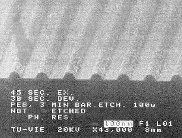
Fig. 6: Photoresist grating analyzed by electron beam microscopy.
The grating consists of positive photo resist, later used for
wet chemical etching.
Image Reversal Resist AZ 5206
The image reversal resist AZ 5206 is suitable for fabrication
of gratings with periods under 500 nm and subsequent lift off
processes. The side walls of this resist form undercut edges and
are therefore not suitable for wet chemical etching. On the other
hand wet chemical etching is known not to be appropriate for such
small structures, since the etchant cannot reach the substrate
due to surface tension. The etching mechanism used with this resist
is ion milling. A grating period of 425 nm with steep side walls
is achieved with the optimized parameters following:
- HCl dip.
- Spin coating with diluted resist AZ 5206 (1:1 with AZ 1500)
for 35 s at 10000 rpm. This corresponds to a resist thickness
of about 500 nm.
- Pre-exposure bake for 60 s at 100°C.
- Exposure by laser for 530 s.
- Post-exposure bake for 60 s at 130°C.
- Flood exposure for 10 s with ultraviolet light.
- Development for 25 s with AZ 726 MIF.
- Post bake for 45 s at 140°C.
- Ion milling etching for 10 minutes at 20° incidence.
This corresponds to an etched depth of 110 nm with steep side
walls.
The fabrication process is very sensitive to exposure time, post-exposure
bake, flood exposure and developing time. To produce smaller periods
with image reversal resist the exposure time should be kept shorter
and the flood exposure must be longer to achieve a one to one
duty ratio. Figure 7 shows an etched grating processed as described
above.
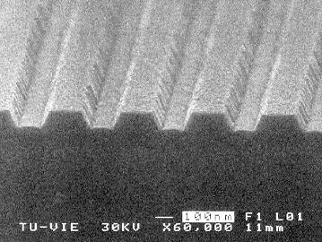
Fig. 7: Surface grating etched by ion milling.
Conclusion
EBL was used to produce arrays of quantum wires for transport
measurements showing interference effects between carriers emerging
out of adjacent wires. Single wires fabricated by EBL were used
for high field measurements. Technology for air bridged Schottky
contacts to be used in THz diodes has been developed. Surface
gratings for emitting laser diodes have been optimized using parts
of the EBL system.
References
[1] M. Hauser, G. Strasser: "Elektronenstrahllithographie
von niedrigdimensionalen GaAs/AlGaAs-Heterostrukturen”, proceedings
Fortbildungsseminar: Grundlagen und Technologie elektronischer
Bauelemente, Großarl 1995, ISBN 3-901578-01-3.
[2] C. Resch, J. Lutz, F. Kuchar: "Transport in AlGaAs/GaAs-Quantendrähten
in hohen elektrischen Feldern”, proceedings Fortbildungsseminar:
Grundlagen und Technologie elektronischer Bauelemente, Großarl
1995, ISBN 3-901578-01-3.
[3] A. Köck, S. Freisleben, C. Gmachl, A. Golshani, E. Gornik;
M. Rosenberger, L. Korte: "Single-mode surface-emitting laser
diodes based on surface mode emission”, Vortrag, Photonics
West, OE/LASE'96, 27. January - 2. February 1996, San Jose,
CA, USA, 1996.
[4] A. Köck, S. Freisleben, C. Gmachl, A. Golshani, E. Gornik;
M. Rosenberger, L. Korte: "Single-mode surface-emitting laser
diodes based on surface mode emission”, Proceedings Nr. 2682,
Laser Diodes and Applications II of Photonics West, OE/LASE'96,
USA, SPIE Optical Engineering Press (1996).
Project Information
Project Manager
Mag. Dr. Gottfried STRASSER
Institute of Solid State Electronics, Technical University of
Vienna, Floragasse 7, A1040 Vienna
Project Group
Last Name      First Name     Status              Remarks

Strasser       Gottfried      postdoc

Hauser         Markus         postdoc             75% GMe funding

Ploner         Guido          dissertation

Zotl           Ernst          student

Köck           Anton          postdoc

Golshani       Alirezah       student

Gornik         Erich          full professor
Presentations
- M. Hauser, G. Strasser: "Elektronenstrahllithographie
von niedrigdimensionalen GaAs/AlGaAs Heterostrukturen”, oral
paper at Fortbildungsseminar: Grundlagen und Technologie elektronischer
Bauelemente, Großarl 1995, ISBN 3-901578-01-3
Diploma Theses
- E. Zotl: "Elektronenstrahllithographie für THz Bauelemente
und Antennenstrukturen”, in progress.
Cooperations
- Dr. Josef Lutz, Prof. F. Kuchar, Montanuniversität Leoben,
Austria
- Dr. Roland Kersting, Institute of Physical Chemistry, University
of Vienna, Austria
- Prof. M. Heiblum, Weizmann Institute of Science, Israel
- Prof. J. Walker, Laboratorio TASC, Italy