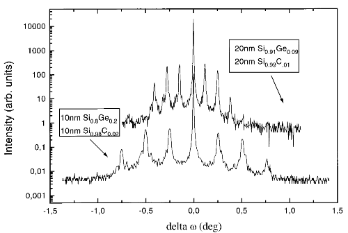
Fig. 1: X-Ray rocking curves of two SiC/SiGe superlattices on (001) Si, which show strain compensation for the parameters (SiGe, SiC layer thicknesses and C and Ge contents as chosen). Number of periods: 10
The molecular beam epitaxy of Si/SiGe, Si/Si1-yCy, and SiGe/Si1-yCy structures is described. The epilayers, heterostructures and superlattices are characterized by high resolution x-ray diffraction using rocking curves, reciprocal space mapping and x-ray reflectivity. In particular it is shown that the strain relaxation mechanism proceeds in the SiC layers via the formation of b-SiC precipitates in contrast to Si/SiGe where misfit dislocations relief the misfit strain. First attempts for a modulation doping of Si/Si1-yCy heterostructures are described, for realizing high mobility two dimensional electron gases. The luminescence from multi-quantum well structures with electrons confined in the Si1-yCy wells was observed and analyzed. In addition, the fabrication and the performance characteristics of Si/SiGe MQW intersubband detectors are described.
Si-based heterostructures offer interesting possibilities for high frequency devices based on Si technology. There has been an increasing interest in such devices and several companies have recently announced the production of Si/SiGe heterobipolar transistors [1].
The MBE growth of Si1-xCx epilayers has recently attracted considerable attention, offering an alternative and addition to the so far much more studied Si/SiGe heterostructure system [2]. Since the lattice constant of these alloys is smaller than that of Si, the epilayers are under biaxial tensile strain, which leads to a conduction band alignment according to which the electrons will be confined to the Si1-xCx layers. Thus, a two dimensional electron gas can be realized in principle within a pseudomorphically grown epilayer. In Si/SiGe heterostructures, such a 2D electron channel can only be realized by depositing a Si layer on top of a relaxed SiGe buffer layer. The necessary relaxation of the SiGe buffer is caused by misfit dislocations and the accompanying threading dislocations penetrate through the active 2D channel to the surface, and are thus unavoidable. This disadvantage is circumvented in Si/SiC heterostructures, at the expense that the 2D electrons are confined in the Si1-xCx layer where they suffer from alloy scattering.
However, the solubility of carbon in silicon is only 3.5x10¹⁷ atoms/cm3 in thermodynamic equilibrium. Non-equilibrium techniques like plasma enhanced chemical vapor, deposition molecular beam epitaxy (MBE) and solid phase epitaxy allow the growth of Si1-xCx epilayers with carbon contents of a few percent (up to about 4%) [3]. We have grown such layers using MBE, where the chamber was equipped with three electron beam evaporators, for Si, Ge, and C. The beam fluxes were monitored and controlled with a quadrupole mass spectrometer, the Si substrate temperatures were varied between 700 °C and 450 °C.
We have investigated the structural quality of such heterostructures, multiquantum wells and superlattices by using several x-ray techniques: (i) high resolution x-ray diffraction, (ii) reciprocal space mapping, (iii) specular x-ray reflectivity measurements and (iv) reciprocal space maps around the origin (000), measuring diffusely scattered radiation. The purpose of these investigations was to assess the strain status of the epilayers, to determine the layer thicknesses and the carbon contents, and to establish whether the deposited epilayers were pseudomorphic or not with respect to the (001) Si substrate. In Fig. 1, rocking curves of two pseudomorphic SiC/SiGe superlattices are shown. The reflectivity measurements yielded information on the Si/Si1-xCx interface roughness as well as the correlation properties within the growth plane and perpendicular to it.
Fig. 1: X-Ray rocking curves of two SiC/SiGe superlattices on (001) Si, which show strain compensation for the parameters (SiGe, SiC layer thicknesses and C and Ge contents as chosen). Number of periods: 10
The main results are the following:
With increasing epilayer thickness and/or with increasing carbon content, the relaxation of the Si1-xCx epilayers occurs through the formation of b-SiC precipitates and not through the formation of misfit dislocation as in the case of Si/SiGe heterostructures.
The epilayers stay pseudomorphic even after the formation of Si1-xCx has occurred as can be determined without any ambiguity from reciprocal space maps around oblique (224) reciprocal lattice points. Apparently, the excess carbon that cannot be accommodated as a diluted alloy forms these precipitates, which have a size from about 2 to 6 nm (as determined by transmission electron microscopy).
The interface roughness of Si/Si1-xCx heterostructures with C contents of about 1 - 2 % is quite similar to that of Si/SiGe heterostructures as has been determined recently by high reflectivity measurements using synchrotron radiation at the Optics Beam Line of the ESRF, Grenoble. (A carbon content of about 1% causes the same absolute amount of biaxial strain as a Ge content of 9%.) In Fig. 2 data on the diffuse scattering are shown, by measuring w-scans in the reciprocal lattice around (000) through the 1st, 2nd and 3rd satellite maximum. Fits to the experimental data as shown yield an interface roughness of about 4Å.
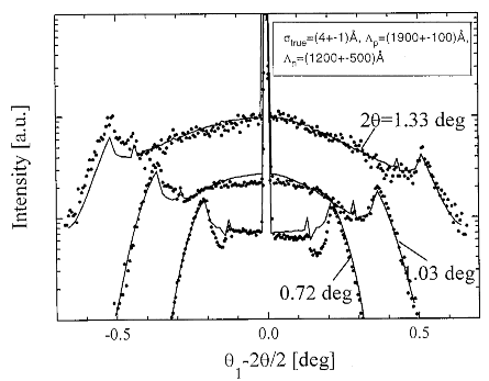
Fig. 2: Determination of interface roughness of SiGe/SiC superlattices from w-scans in the reciprocal lattice.
We have also investigated the thermal stability of such heterostructures by thermal annealing experiments at temperatures in the range from 800° to 950°C. The thermal treatment causes also the formation of ß-SiC precipitates, whereas the remaining carbon stays substitutionally on Si sites in the lattice. Thus the annealed Si1-xCx epilayer stays pseudomorphic, but annealing reduces its carbon content at the expense of precipitate formation. Even at these elevated temperatures used for the annealing experiments no evidence for misfit dislocation formation was found within the accuracy of the x-ray mapping methods.
For the use of Si/Si1-xCx heterostructures the findings about the interface roughness are encouraging for future devices. The annealing experiments show that the thermal stability of the silicon-carbon alloys is comparable to that of SiGe alloy layers, with the main difference that no misfit dislocation formation occurs.
There is a strong need for infrared detectors operating in the two atmospheric windows at 3 - 5 mm and 8 - 12 mm which are based on silicon and are thus compatible with existing Si electronics. Presently silicide (PtSi and IrSi) detectors are employed for imaging arrays, whereas HgCdTe is used for high-sensitivity single-element applications. Quantum well infrared photodetectors (QWIPs), which are based on intersubband transitions in quantum wells, are promising alternatives which ultimately could replace both of the above. Up to now, most of the related research has concentrated on GaAs/ AlGaAs quantum wells [4]. In the present report we describe the fabrication and performance of QWIPs based on Si/SiGe quantum wells [5].
The detector structures consist of 10 Si0.65Ge0.35/Si quantum wells with a thickness of 25 Å, separated by 300 Å Si barriers and are grown pseudomorphically on a Si (001) substrate. The quantum wells were doped p-type to 1.2 x 1012 cm-2 per well. The active region is enclosed by two heavily p-doped contact layers. The quantum well thickness is such that the first excited heavy-hole state is near the top of the quantum wells, so that the absorption of an infrared photon leads to a photocurrent.
The samples were characterized by polarization dependent infrared absorption spectroscopy, which allowed clear assignment of the active transitions [6]. The cut-off wavelength of the present structure is at 1200 cm-1 (8 mm) for p-polarized and at 1400 cm-1 (7 mm) for s-polarized radiation. s-polarized absorption, which is equivalent to normal-incidence absorption, is only possible due to the band mixing present in the valence band. This is a significant advantage when compared, e.g., to n-GaAs QWIPs, where normal-incidence detection is not possible without special coupling schemes. In our device the photoresponse between 3 mm and 7 mm peaks at a wavelength of 5 mm and is actually higher in s-polarization than in p-polarization.
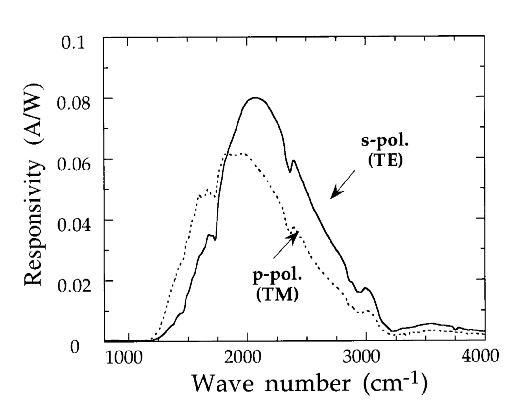
Fig. 3: Spectral dependence of the photoresponse measured in s- (solid line) and p-(broken line) polarization.
Detector elements of 100 - 400 mm diameter were fabricated by photolithography, reactive ion etching and metal evaporation/lift-off techniques. The spectral dependence of the responsivity for both orthogonal polarization directions is shown in Fig. 3. Figure 4 shows the dependence of the normal-incidence responsivity on the bias voltage, V. At V = -3.5 V, we measure a normal-incidence current responsivity as high as 80 mA/W.
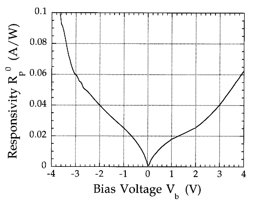
Fig. 4: Bias dependence of the peak responsivity.
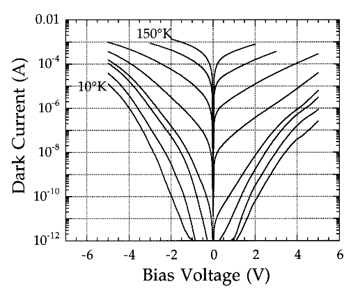
Fig. 5: Dark-current-voltage characteristics of a 200 mm mesa device for temperatures between T = 10 K and 150 K, in steps of 20 K.
In Fig. 5, the dark-current-voltage characteristics of a 200 mm device are shown for temperatures between T = 10 K and 150 K, in steps of 20 K. If the dark current divided by the temperature is plotted versus the inverse temperature, an activation energy can be extracted. Such an evaluation is presented in Fig. 6. At V = 1 V, an activation energy of 154 meV results, which is consistent with the energy difference between the Fermi level and the top of the barriers in the present structure. At higher bias, the activation energy decreases due to the effective lowering of the barriers (not shown). The low dark current gives rise to BLIP (background limited infrared performance) operation at T = 80 K for a bias of 1 V and even higher BLIP temperatures at lower bias. Noise measurements for evaluation of the detectivity, D*, are currently performed.
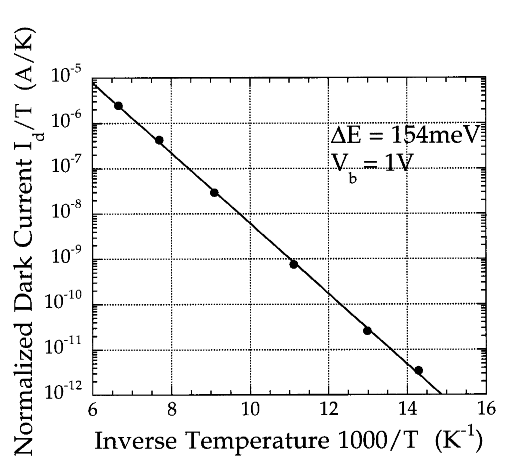
Fig. 6: Evaluation of the activation energy from the dark current at 1 V bias voltage.
To summarize, we have shown that high-performance normal-incidence QWIPs can be fabricated from Si/SiGe. Such detectors can be designed for different peak wavelength over a wide range and are more sensitive than silicide detectors.
As described in the proposal, a facility for photoluminescence measurements in the near infrared has been set up in Linz. The Si based heterostructures are excited with Ar-ion laser radiation, and the samples are placed in a variable temperature insert in a He cryostat. The luminescence light is collected and analyzed with a grating monochromator and detected with a North Coast Ge detector. A wavelength range from 0.8 mm to 1.7 mm can be covered with this system.
The luminescence studies contribute essentially to the characterization of the MBE grown materials, in particular the luminescence lines and their efficiency yield information on the amount of defects present.
The luminescence from Si/SiGe quantum wells grown pseudomorphically on (001) Si has been well described in the literature. A series of such MQW's with the following parameters 10 x (51.3 Å SiGe0.23 / 69Å Si), 10 x (68Å SiGe0.31 / 61Å Si), 10 x (30.8 Å SiGe0.23 / 69 Å Si) has been measured and is shown in Fig. 7. The spectra are dominated in the SiGe QW-part by the no-phonon line (NP) and the Si-Si TO phonon replica line. These structures shift with decreasing quantum well width to higher energies. Furthermore, at about 1.1 eV a series of luminescence lines appears which are due to radiative band edge recombination in the Si layers (TO phonon replicas of free excitons and bound excitons due to boron impurities). At 1.15 eV the no-phonon band edge recombination lines of Si appear.
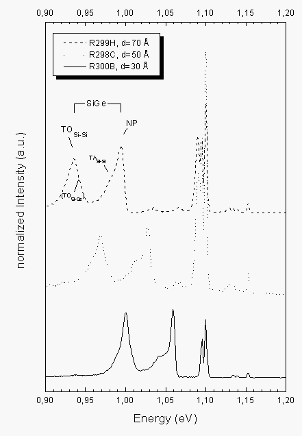
Fig. 7: Measurements on SiGe MQWs, normalized to the SiGe-NP signal. The samples have different quantum well widths, one can clearly see the increase of the confinement-energy with decreasing well width.
Recently, Eberl et al. [7] have concluded from luminescence studies on a series of Si/Si1yCy multi-quantum wells that this system has a type I band alignment, which would make these heterostructures extremely interesting for optoelectronic applications. However, there is still a controversy about the interpretation of these data regarding conclusive evidence for a type I band alignment.
We have recently performed preliminary investigations on the luminescence from our MBE grown Si1-yCy epilayers, on Si/Si1-yCy quantum wells and multiquantum well structures. In Fig. 8, the luminescence vs. energy is shown for a Si/Si1-yCy multi-quantum well (MQW) sample with a carbon content in the wells of 1.5%, a well width of 50 Å, a Si spacer width of 150 Å (10 periods). In the photoluminescence spectra a no-phonon line and a TO phonon replica from the Si1-yCy quantum wells can be seen at about 1.04 and 0.98 eV. The lines at higher energies are due to electron-hole droplets (1.08 eV), the TO-phonon replica of a bound exciton line at 1.092 eV and finally the no-phonon bound exciton line of Si at 1.15 eV. This sample was grown at about 450°C.
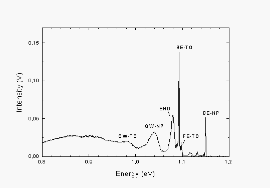
Fig. 8: Photoluminescence spectrum from a Si/Si1-yCy MQW.
In order to grow strain compensated structures on the (001) Si substrates, a MQW structure with alternating Si1-xGex and Si1-yCy layers can be grown. Luminescence data from such a MQW with Si1-xGex (x = 9.15%) layer thicknesses of 87 Å and Si1-yCy (y = 1.37%) of 87 Å are shown in Fig. 9. The luminescence efficiency is smaller than for Si/Si1-yCy quantum wells, however a transition at 1.115 eV and its TO replica at 1.055 eV are attributed to QW luminescence. All other lines originate from Si.
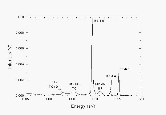
Fig. 9: Photoluminescence spectrum from a strain-compensated Si1-xGex/Si1-yCy MQW.
The rather weak luminescence from the QW regions in the Si1-xGex/Si1-yCy MQW's is most probably not an intrinsic property of the strain compensated Si based heterostructures but reflects rather insufficient material quality. In particular, the fact that free exciton lines are absent and only bound exciton lines (due to Sb or P) can be seen indicates rather high unintended impurity concentrations. Modifications of the e-beam evaporators scheduled for the next two months and additional pumping of the growth chamber by a newly commissioned turbo pump are expected to greatly improve the background contaminations in the MBE apparatus.
Si /SiGe and Si/SiC heterostructures have been grown by MBE and characterized with respect to their structural, electronic, and optical properties. The structural characteristics of pseudomorphic Si/SiC heterostructures are quite similar to those of Si/SiGe, in particular with respect to the interface roughness. First experimental data on modulation doping of Si/SiC structures have been obtained. An electron mobility enhancement with respect to that of bulk Si has been observed in SiC channels, however, mobilities are still influenced by background residual impurities. Interband luminescence in Si/SiC quantum wells was observed as well.
Intersubband quantum well detectors (Si/SiGe MQW's) for the mid-infrared region were fabricated and characterized with respect to their detector characteristics.
This work has been supported apart from the GMe by the Fonds zur Förderung der wissenschaftlichen Forschung, Vienna, by the Projektförderung Bundesministerium für Wissenschaft und Forschung, Vienna, as well as by ESPRIT basic research action "UMIST".
[1] E. Kasper and F. Schäffler, Semiconductors and Semimetals, eds.R.Wiilardson and A. C. Beer (Academic Press, San Diego, 1991) Vol.33, p.231.
[2] K. Eberl, S. S. Iyer, and F. K. Le Goues, Appl.Phys.Lett. 64, 739 (1994).
[3] H. Rücker, M. Methfessel, E. Bugiel, and H. J. Osten, Phys.Rev.Lett. 72, 3578 (1994).
[4] B. F. Levine, J. Appl. Phys. 74, R1 (1993).
[5] R. People, J. C. Bean, C. G. Bethea, S. K. Sputz, and L. J. Peticolas, Appl.Phys. Lett. 61, 1122 (1992).
[6] T. Fromherz, P. Kruck, M. Helm, G. Bauer, J. F. Nützel, G. Abstreiter, Superlattices and Microstructures, in print.
[7] K. Brunner, K. Eberl, and W. Winter, Phys. Rev. Lett. 76, 303 (1996).
Univ.-Prof. Dr. Günther BAUER
Institut für Halbleiterphysik, Johannes Kepler Universität Linz, A-4040 Linz, Austria
Last Name      First Name     Status              Remarks

Bauer          Günther        Professor

Schäffler      Friedrich      Professor

Helm           Manfred        Univ.-Doz.

Brunthaler     Gerhard        Ph.D.

Faschinger     Wolfgang       Univ.-Doz.

Fromherz       Thomas         postdoc

Darhuber       Anton A.       dissertation

Kruck          Peter          dissertation

Penn           Christian      dissertation

Stangl         Julian         dissertation

Straub         Hubert         dissertation        50% GMe funding

Zerlauth       Stefan         dissertation