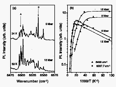
Fig. 1: (a) Photoluminescence of Si:Er, O without and with a hydrostatic pressure of 12 kbar. (b) Arrhenius plot of the luminescence intensity of two lines marked in Fig. 1a (circle and triangle, respectively) with and without pressure.
We present two examples of current investigations of point defects in semiconductors: (i) the characterization of Er centers in Si and their properties as a source of 1.5 µm luminescence, and (ii) problems arising in the doping of large gap II-VI compounds. We show that the luminescence yield of Er in Si can be improved by hydrostatic pressure, and we explain this in terms of energy transfer via defect recombination. Nitrogen in II-VI compounds is shown to be an effective acceptor as needed for light emitters from such materials.
The controlled introduction of point defects with well-known structural, electronic and thermodynamic properties is the most important tool for the achievement of specific properties and thus for the fabrication of semiconductor devices. In spite of 50 years of intense research on the properties of point defects in semiconductors there is still a number of barely understood problems. Two of such problems are investigated here.
The first one concerns erbium as a dopant in silicon. The rare earth element erbium has an incompletely filled inner 4f shell that is very well shielded by the outer 5th and 6th shell. The crystal rather acts as a weak perturbation and the radiative internal transitions within the 4f shell produce almost atom-like spectra with the main transition occurring at 1.54 µm, independent of the host crystal [1 - 3]. The latter manifests itself only by its crystal field, which, together with other nearby defects and impurities, causes subtle characteristic splittings of the main transition. Nevertheless, owing to the long radiative life time of about one millisecond and the weak perturbation, the line widths are extremely narrow (typically less than 0.1 cm-1) and the splittings are well resolvable.
The wave length of the main transition, 1.54 µm, makes Si:Er an interesting candidate for a Si-based integrable light source for optical communication via silica fibers, which have their minimum damping right at that wave length. Problems arise, however, from the temperature induced quenching of the luminescence yield, which occurs well below room temperature already. Co-doping with light elements like C, N, F, and, most efficiently, O, was found to improve the efficiency dramatically but still not sufficiently for room temperature applications. In this work, we show another way of improving the efficiency by application of hydrostatic pressure. We attribute this effect to the change in the energy transfer rate from the Si crystal to the 4f shell of the Er, whereby we consider the role of additional oxygen as co-activator in the Er luminescence.
In part 3 of this report we describe our efforts and successes in the attempt to dope large gap II-VI compounds also highly p-type. The latter is a necessary requirement for laser structures built from such materials with the goal of achieving short wave length emission.
The originally rather weak PL yield has been substantially improved over the years by co-doping with light elements and optimized annealing procedures, without gaining too much insight in the underlying physical mechanisms [2]. In particular, the question, how the energy is transferred from the host crystal to the 4f shell of Er, which produces this PL, is only tentatively solved.
Most authors assume that defects are involved in this process. In a first step, the exciting photon is absorbed and generates an exciton that can transport part of the excitation energy over macroscopic distances, much wider than the Er-containing surface layer that is produced either by ion implantation or molecular beam epitaxy. (These techniques are preferred since they produce a state far from thermal equilibrium and thus they allow to overcome the limited solubility of Er.) Then these excitons are trapped at or close to an Er containing defect located close to the surface. As a next step, the de-excitation or recombination of the exciton leads to a non-radiative transfer of the necessary energy for the intra-4f transition from the J = 15/2 ground state to the first excited, the J = 13/2 state. Obviously, different Er configurations have different efficiency in this transfer process, which allows to optimize the PL yield by "breeding" particularly suitable Er complexes by co-implantation and short time annealing procedures [3].
The energy released by the "supplying" defect state should be at least close to the intra 4f excitation energy. A difference in energy can be accommodated by local phonons or other low energy excitations. The latter process works better at elevated temperature which causes, however, also a quenching of the PL yield due to a "backtransfer" process which is envisioned as just opposite to the excitation process: under thermal excitation, the exciton bound at the supplier defect can be released again and dissipated elsewhere.
In order to test such a model, we have performed a study of Er in Si under hydrostatic pressure. High resolution Fourier spectroscopy allows us to distinguish different centers as reviewed elsewhere [3] and to determine their PL yield individually up to temperatures of well above 200 K. The sample is put into a pressure cell employing a piston and benzene as pressure transmitting medium up to a pressure of 20 kbar. The cell is attached to a cold finger cryostat and cooled to temperatures down to 10 K.
In Fig. 1 (a), two PL spectra of Si:Er, O are shown for 0 and 12 kbar, respectively. It is clearly seen that pressure affects different lines that belong to different centers individually: some lines increase strongly, some decrease and others seem to be unaffected. The dependence of the PL intensity for the two lines indicated in Fig. 1 (a) by arrows on temperature is given in Fig. 1 (b) for the two pressures of 0 and 12 kbars each.
Fig. 1: (a) Photoluminescence of Si:Er, O without and with a hydrostatic pressure of 12 kbar. (b) Arrhenius plot of the luminescence intensity of two lines marked in Fig. 1a (circle and triangle, respectively) with and without pressure.
This type of behavior is observed only in samples with additional oxygen implantation as shown in Fig. 2: here the normalized intensity of the same cubic center is shown with and without pressure, with and without additional oxygen. Only after oxygen implantation the beneficial effect of the hydrostatic pressure is observed.
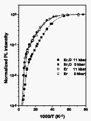
Fig. 2: Arrhenius plot of the luminescence intensity of Si:Er, O (full symbols) as compared to that of a sample without additional O implantation.
We may conclude from these findings that apparently oxygen provides an additional path for the energy transfer from the Si crystal to the Erbium 4f shell. This additional transfer mechanism depends obviously strongly on pressure. In the case of the cubic Er center and one of the centers ascribed earlier to an Er-intrinsic defect complex named "D1" the pressure causes an increase in intensity by almost an order of magnitude in an intermediate temperature regime (140 K > T > 25 K).
In an earlier paper [3] we have considered energy transfer via bound excitons which yields expressions of the type:
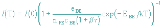
where eBE, EBE, cBE stand for the emission rate, the binding energy and the capture rate of excitons, b for the transfer coefficient and t for the Er radiative life time. Fitting such expressions (two separate ones for the regimes T < 100 K and T > 120 K) to the observed temperature dependence under pressure shows that in the intermediate temperature regime the activation energy is independent of pressure but the prefactor, which contains the coupling coefficient b, is strongly affected. In order to explain this behavior we propose that in the case of the additional transfer mediated by oxygen excitons trapped at oxygen centers excite first an oxygen-related deep level, which, in turn, transfers its excitation energy to the 4f shell of Er.
The effect of pressure is to shift the oxygen level relative to the 4f excitation energy. This mechanism explains the strong pressure dependence of b, which, in the spirit of perturbation theory, is described in terms of matrix elements and energy difference denominators. The latter may account for the observed strong influence of hydrostatic pressure on the PL yield, whereas the activation energy for quenching remains unchanged. This activation energy corresponds in our picture to the detachment energy of the bound exciton. Bound excitons are rather extended states, and these are well known to exhibit rather small pressure coefficients.
The observation of the strong influence of pressure on the PL yield thus suggests a new mechanism for the energy transfer and thus it also explains the beneficial role of oxygen-co-doping on the luminescence yield of Erbium in Si. This mechanism suggests also new possibilities to improve the efficiency of Si:Er based light emitting devices.
The successful fabrication of the first blue-green laserdiodes in 1991 caused a breakthrough in the technology of the II-VI compound semiconductors with large energy gap. Lasers emitting in the blue range are needed, for example, for optical data storage at higher density than present. The main problem, namely the p-type doping of ZnSe, was solved using activated nitrogen as an acceptor.
Contemporary laser structures contain in the active region a so-called quantum well consisting of ZnCdSe with about 20% CdTe, corresponding to an energy gap of 2.54 eV at low temperatures. In order to extend the wave length further to the blue range an energy gap of 2.65 eV is needed for the active region. This requirement implies, however, that the gap of the cladding layers, consisting of ZnMgSe, should exceed 3 eV in order to provide the necessary optical and electrical confinement. The hole concentration then is limited, however, to less than 4 x 1016 cm3 for a gap of 3.05 eV. This low value would lead to an enormous increase in the threshold voltage, which would further enhance degradation. The main task therefore was to find a material with both a large energy gap and higher saturation carrier concentration.
New doping techniques in molecular beam epitaxy based on plasma-activated N2 gave carrier concentrations for p-type material orders of magnitude higher than previously obtained doping levels. Another milestone was the incorporation of magnesium into the family of II-VI compounds. In that way the energy gap and the lattice constant can be chosen separately in the quaternary compound.
In the framework of the research project supported by the GMe, the material system ZnMgSeTe was investigated and first electroluminescent devices were fabricated based on that quaternary compound. The epitaxial layers were grown in an MBE chamber equipped with effusion cells for Cd, Zn, Mg, Se, Te, and additional chlorine and nitrogen sources for n- and p-type doping. The most important results obtained in this field are the following:
The first diode, realized in this material system, emitted in the green spectral range and showed electrical properties comparable with LEDs fabricated by Sony in 1994. With a forward bias of 6 V a current density of 500 A/cm2 is obtained, which is clearly above the threshold current for laser emission. By using a ZnMgCdSe multi-quantum-well structure, the wavelength of the emitted light could be shifted into the deep blue spectral range.
Besides the excellent electrical characteristics of our LEDs there are some drawbacks in the linewidth of the emitted light, which made laser activity impossible so far.
One of the main reasons for that was the fact that our LEDs were grown on GaAs substrates and 2.5 mm thick buffer layers of ZnMgSe. That means that the whole structure contains much lattice mismatch causing dislocations at interfaces and as a consequence, it broadens the linewidth of the optical emission.
We thank H. Heinrich for his continuous interest in this work and A. Polman (FOM Amsterdam) and J. Langer (PAN, Warsaw) for helpful discussions.
[1] H. Ennen, G. Pomrenke, A. Axmann, K. Eisele, W. Haydl, and J. Schneider, Appl. Phys. Lett. 46 (1985), 381.
[2] J. Michel, F.Y.G. Ren, B. Zheng, D.C. Jacobson, J.M. Poate, and L.C. Kimerling, Materials Science Forum 143 - 147 (1994), 707.
[3] H. Przybylinska, W. Jantsch, Yu. Suprun-Belevich, M. Stepikhova, L. Palmetshofer, G. Hendorfer, A. Kozanecki, R. J. Wilson, B. J. Sealy: "Optically active Erbium centers in Silicon", Phys. Rev. B, submitted.
Univ.-Prof. Dr. Helmut HEINRICH
Institut für Experimentalphysik, Johannes Kepler Universität, A-4040 Linz
Last Name      First Name     Status              Remarks

Jantsch        Wolfgang       ao.Prof.

Palmetshofer   Leopold        Univ.-Doz.

Sitter         Helmut         Univ.-Doz.

Przybylinska   Hanka          Dr.                 Inst.Physics, Polish
                                                  Academy of Sciences,
                                                  Warsaw

Lanzerstorfer  Sven           dissertation        16% GMe funding

Schmidt        Thomas         dissertation        10% GMe funding

Stifter        David          dissertation        10% GMe funding

Vaskovich      Lore           technician          33% GMe funding