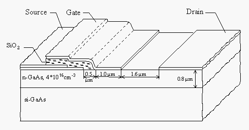
Fig. 1: Cross-sectional view of the FECTED
Experimental results achieved with planar GaAs transferred electron oscillators at V-band frequencies are reported in this contribution. The active devices are MESFET-like structures with a Schottky-gate controlling the electron injection into the drift region. The electron injection is adjusted to a level yielding a frequency independent negative differential resistance, which is exploited for millimeter-wave power generation. The highest measured CW output power and efficiency are 8 mW and 1.6 % at 59.5 GHz, respectively. These results are comparable to those obtained with transistor oscillators which are much more difficult to fabricate due to their extremely small dimensions in the 0.1 µm range.
Millimeter-wave MMIC´s have potential of being extensively used in future industrial and communication systems. In these systems one of the key elements is the oscillator capable of producing enough output power at these high frequencies. For power levels above 10 dBm at millimeter-wave frequencies mostly two-terminal devices such as Gunn or IMPATT diodes are used. The power levels achieved with transistor oscillators are lower than those of two-terminal devices but transistor amplifiers can be used for boosting up the power levels and they are in general much better suited for monolithic integration. Their disadvantage is the highly sophisticated technology needed to fabricate these millimeter-wave transistors.
A device much easier to fabricate is the so called Field Effect Controlled Transferred Electron Device (FECTED) which combines the simplicity of two-terminal devices with the ability of being integrated with transistors and diodes. The FECTED is basically a planar Gunn-diode with an injection limiting cathode contact [1]. Due to the limited electron injection of the cathode the transit-time limitation is removed which makes the device especially well suited for millimeter-wave power generation. The main advantage, however, is the relaxed geometry of the device so that easy fabrication is possible. Very impressive results have been obtained at 35 GHz [2]. We now report new results achieved with identical devices operated at V-band frequencies.
Figure 1 shows a cross sectional view of a typical device. It consists of an 0.8 µm thick MOCVD-grown n-doped GaAs channel layer with a doping level of about 4*1016 cm-3, an alloyed Ni-Au-Ge ohmic source contact, a Cr-Au-Schottky drain contact and a Schottky gate. A Schottky drain contact instead of an ohmic one has been used in order to keep the electric field there low thereby minimizing breakdown effects [3]. The overlapping Schottky gate is separated from the source contact by a chemical vapor deposited SiO2 layer with a thickness of 500 nm connecting the gate to ground RF-wise. The device width is 200 µm and the thickness of the semi-insulating substrate is 150 µm. The device as well as the circuit layout (Fig. 2) has been defined by electron beam lithography.

Fig. 1: Cross-sectional view of the FECTED

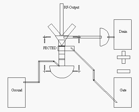
Fig. 2: Layout of the circuitry of the 60 GHz oscillator
At 59.5 GHz an output power of 8 mW with an efficiency of 1.6 % has been obtained. The output power was corrected for the losses in the waveguide-to-microstrip transition and the measurement setup. Drain voltage and current were 7.5 V and 66 mA, respectively. The measured phase noise was about -78 dBc/Hz @ 1 MHz off carrier. A useful modulation range of about 1 GHz was obtained by simply changing the negative gate bias voltage. The highest frequency obtained with this design was 63.8 GHz with an associated power level of 1.76 mW and an efficiency of 0.43 %. Although these results have been achieved with circuits designed without any extensive simulations or CAD tools, they are nevertheless comparable to those achieved with transistor oscillators [4], [5].We therefore believe that improved performance should be obtainable by introducing more rigorous modeling and better testing equipment. Also, the use of a composite anode contact that combines a short stripe of a Schottky metal with an ohmic contact should lead to further improvement of performance [3].
Planar, monolithically integrated transferred electron oscillators have been fabricated for operation at V-band frequencies. The active device is a planar Gunn-diode with an injection limiting cathode contact that exhibits a broad band negative differential resistance, which is used for millimeter wave power generation. This device, which is called FECTED (Field Effect Controlled Transferred Electron Device), is easy to manufacture and has a simple circuitry because it is a two-terminal device. The best result obtained with this type of oscillator is 8 mW at 59.5 GHz with an efficiency of 1.6 %. It is believed that further optimizations by means of better modeling and testing could result in higher power levels as well as in better efficiency.
The authors would like to thank G. Hinterberger, G. Hofmann and J. Katzenmayer for fabricating and testing the devices. This work was supported by the Austrian Science Foundation (FWF) under contract number P8697 - TEC.
[1] H. Scheiber, K. Lübke, D. Grützmacher, C. G. Diskus, H. W. Thim: "MMIC Compatible GaAs and InP Field Effect Controlled Transferred Electron Device (FECTED) Oscillators", IEEE MTT, Vol. 37, No. 12, p. 2093 - 2098, Dec. 1989.
[2] C. G. Diskus, K. Lübke, A. L. Springer, H. W. Lettenmayr, H. W. Thim: "Abstimmbarer GaAs Oszillator MMIC", Conference Proceedings, MIOP ´93, Sindelfingen, p. 151 - 155.
[3] C. G. Diskus, A. L. Springer, K. Lübke, H. W. Lettenmayr, H. W. Thim: "Composite Anode Contact for Planar Transferred Electron Devices", IEEE Microwave and Guided Wave Lett., Vol. 3, No. 6, pp. 180 - 181, June 1993.
[4] U. Güttich, J. Wenger: "Design, Fabrication and Performance of Monolithic Dielectrically Stabilized PM-HFET Oscillators up to 60 GHz", Proc. of the 24th European Microwave Conference, Cannes, 5.-8. Sept. 1994, pp. 361 - 363.
[5] A. Bangert, M. Schlechtweg, W. Reinert, W. H. Haydl, A. Hülsmann, K. Köhler: "Monolithic integrated 75 GHz oscillator with high output power using a pseudomorphic HFET", IEEE MTT-S Int. Microw. Symposium Digest, 1994, pp. 135 - 138.
Univ.-Prof. Dr. Hartwig THIM
Institut für Mikroelektronik, Kepler-Universität Linz, Austria
Last Name      First Name     Status              Remarks

Diskus         Christian      postdoc

Hinterberger   Gabriele       technician

Hofmann        Gerald         technician

Katzenmayer    Johann         technician

Lübke          Kurt           postdoc

Springer       Andreas        dissertation

Thim           Hartwig        university
                              professor