Fig. 1: Block diagram of the PCC implementation
After giving a short survey of the project aims of UNICHIP and its development over the last years, selected activities are presented which have been completed in the last year. Besides covering new methods in teaching the design of user programmable logic devices, results of a long year research project on a multiple redundant field bus are described. The last part includes industry related projects. In the past year several analogue and digital ASIC design projects have been accomplished in cooperation with Austrian SMEs.
The UNICHIP project was originally proposed in 1987 by the Institut für Allgemeine Elektrotechnik und Elektronik at the Vienna University of Technology. Since its very beginning this national activity was focused on three main topics in the area of the design of digital and analogue integrated circuits. Firstly, undergraduate education had to be intensified by means of offering the students access to state of the art hard- and software design tools together with the possibility to actually manufacture selected designs. Secondly, effective accomplishment of research and advanced development projects should be made feasible. Finally, the Austrian industry - mainly Small and Medium sized Enterprises (SMEs) - should be supported in using new technologies and design methodologies.
All of these aims required continuous investments in design hardware and Engineering Design Automation (EDA) software tools. Additionally, a measurement lab had to be installed enabling the verification on both digital and analogue behavior of integrated circuits that have been fabricated in the scope of UNICHIP.
The GMe has funded UNICHIP throughout the past years so we were able to set up and operate a ASIC design facility and thereby achieve every one goal of UNICHIP at least to a certain extent within the first years. The participation in the ESPRIT project Teaching VLSI Design Skills (EUROCHIP) and later on in EUROPRACTICE turned out to be a major breakthrough for UNICHIP. Both of these projects were launched by the European community to accomplish similar goals as UNICHIP but on a pan-European level. Several services are available such as very cheap access to both a variety of EDA tools and to IC prototype manufacturing facilities. Education and academic research are showing great success and have been pushed to an advanced level comparable to other European universities. In the recent past the SME support activities - by far the most difficult task - have been successful.
The remainder of the report will cover all three aspects of UNICHIP be means of short descriptions of selected projects.
UPLDs became an eminent factor in industry because of growing available complexity and pin numbers. They offer the advantage of system integration and miniaturization at small volumes. The migration to, for example, a gate array for high volumes is easier to achieve since some parts of the gate array design may be done automatically using special software tools for converting the UPLD design.
The goal of this new course is to teach practical knowledge about the structure, technology, and the area of application of UPLDs. The students gain personal experience by designing selected small circuits and transferring them from one design system or UPLD structure to another and comparing the results.
The course showed a comprehensive overview about all relevant UPLD-device families and their design tools. Not only were technical aspects like structure, speed, and complexity discussed but also economic criteria like availability, support, the structure of costs, and the important industrial aspects like problems with device programming (time, verification, long term stability) and second source were shown. Numerous software and UPLD distributors and manufacturers made test systems available for this course. This engagement enabled an objective comparison of different architectures and software tools.
The fundamentals of UPLDs were taught in five lectures at the beginning of the course. After that each student had to implement some small sample circuits on different architectures with different software tools. It was the intention of the selected examples to show which UPLD family is suitable for a special circuit structure or which software fits for a special design method. The students had to comment, interpret, and compare the obtained results.
It was the new approach of this course to teach UPLD knowledge not only by means of one special family with a selected design system but to present all available architectures and all relevant design systems. This wide approach together with solid fundamentals enables the students to make good use of their knowledge even in four or five years. This is very important due to the fast changes of technology in the UPLD area.
The following UPLD families were taught:
The following CAE-design systems were available:
24 students were registered for the CAE course "Design of User Programmable Logic Devices". 20 of them have successfully finished their works. It was the key work of the examples to implement small designs on different architectures with a minimum of assistance. Therefore, they had to document not only their implementation of the simple example, which is quite boring, but their experiences and a critical comparison of the results with different tools and architectures.
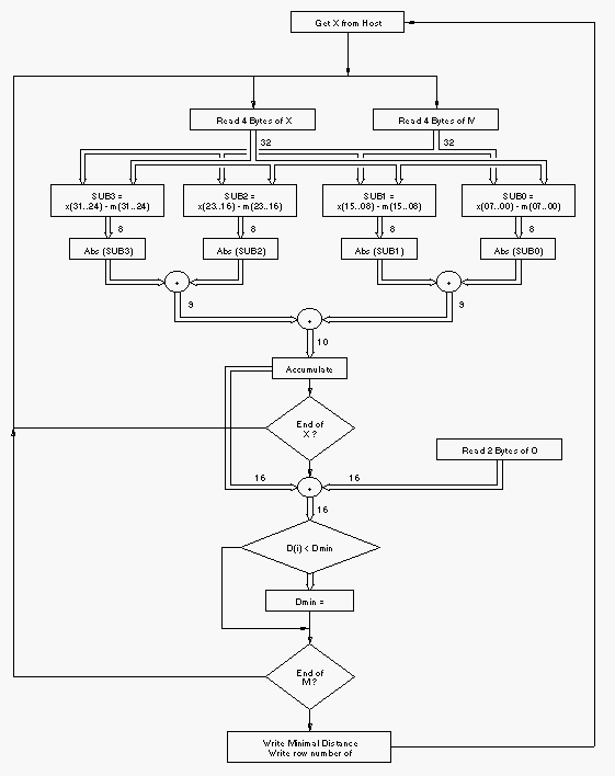
The aim of this project was to speed up a time consuming pattern matching algorithm by implementing it in hardware. The algorithm and system design have been accomplished by our industrial partner. Referring to several years of experience in developing complex UPLDs (User Programmable Logic Devices), the authors were put in charge of designing of a Pattern Classification Subsystem containing hardware accelerators. Besides of a complete specification of the interface circuitry, the PCC was defined as follows: Given a matrix M of size and a vector X of size j, the Manhattan distance between every row of M and X is calculated. The resulting vector is weighted by adding an offset vector and finally the minimal component of this sum is generated and written to the output port of the subsystem together with the corresponding row of M.
Adding all operations necessary to compute the Minimal Weighted Manhattan Distance (MWM) and taking the time constraints into account resulted in a CPU capable of performing some 260 MOPS. Expressed in another way, this leads to a necessary instruction cycle time of less than 4 ns. The first version of the PCC included the Manhattan distance calculation unit for 64 components per vector. The PCC was implemented using a XILINX FPGA (XC-4010) which was the only device available comprising the required resources such as 20 MHz system clock frequency, 16 bit adders with less than 50 ns delay, more than 700 flip flops, and 64 Byte on chip SRAM. Figure 1 shows a flow chart of the algorithm as implemented.
Fig. 1: Block diagram of the PCC implementation
The System was implemented as a full sized PC-AT ISA Bus compatible board with a DSP as an on-board host CPU for the PCC. The PCC Subsystem is a successful implementation of an algorithm in hardware using one high density FPGA to its very extent. Compared to a software version of this algorithm running on a PC we gained computation speed of two orders of magnitude.
The XILINX FPGA has been replaced by a mask programmed version of the device recently, thus reducing the production costs of the complete system.
The transmission line is the most sensitive part of a field bus. Not only do electromagnetic disturbances cause transmission errors, a failure of the transmission medium consequently means the failure of at least parts of the whole communication system. Moreover, repairing a broken cable is far more difficult than the exchange of other system components that are easily accessible. The use of redundant transmission lines is a possible solution, yet most of the existing field bus systems provide no means to facilitate the implementation of fault tolerance.
In contrast, the XR-III field bus makes use of two additional, active redundant cables, which ensures fault tolerance without any supplementary hardware as well as optimal performance. It features a serial master-slave structure suited for sensor-actuator applications, up to 256 nodes connected to a ring, 10 MHz data rate, and identical single-chip-controllers both for master and slave. The transmission medium is left to the choice of the user, fiber optic links are possible as well as coax or twisted pair cables with or without coupling transformers.
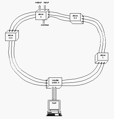
Fig. 2: XR-III structure
Data integrity is obtained basically by a CRC used for detection and correction of transmission errors and improved further using the active redundancy. This means that the data is transmitted simultaneously over all three lines and the receiver compares the information coming in on all lines and finally decides by a majority vote what has actually or more likely been sent. This active redundancy also prevents the loss of data in case of a cable failure.
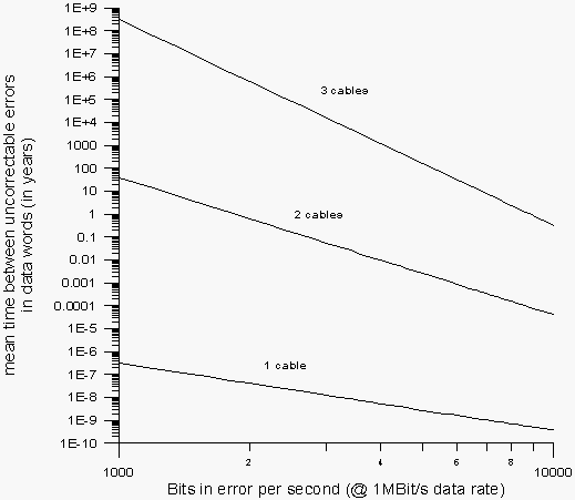
Fig. 3: Performance comparison using 1, 2, or 3 transmission lines
The first step towards realization of the concept was the design of a prototype using FPGAs. To ease implementation, a number of functions were omitted, and the design concentrated on the innovative and essential features of the concept. This way, the concept of active redundancy could be proved to be fully functional in praxis. Subsequently, a hardware description of the ASIC completed in the scope of a diploma thesis as a starting point for the production of a standard cell IC including the complete functionality of the XR-III protocol.
This project was initiated by the Viennese firm IMS who were looking for a Transputer based control hardware for their ion beam lithography machine. The Transputer architecture was selected mostly because of its ability to support distributed real time process control and the availability of high speed serial links. The latter were of particular importance since the whole subsystem was to be operated at a high dc potential (some 100 000 V), which demanded optically isolated data connections to the main computer. As the electrical environment was expected to be very harsh, great care had to be taken concerning EMC and ESD.
The complete subsystem consists of three double Euro printed circuit boards devoted to three distinct tasks. One comprises the Transputer itself, the electro-optical converters for two links that are used to communicate with the outside world, a state-of-the-art UART to interface with high end measurement equipment such as high resolution digital multimeters, two PS2 sockets for up to 8 MByte DRAM SIMs, and 32 optically isolated digital IOs. The connection to the other boards is given through the reserved signals of an off-the-shelf VME-bus backplane.
The second is a twelve-channel DA board for controlling the so-called multipoles that regulate the ion beam. Each channel is made up of a 16-bit DAC followed by an analogue amplifier. An on-board SRAM stores the last values written to the DACs to allow readback and serves as additional external storage facility for the Transputer. Because of the high density of components and to meet the EMC requirements, the board had to be entirely hand-routed. Two of these boards may be cascaded in a master-slave-configuration with a single central voltage reference.
Finally, the third board is used to control two power supplies. It comprises two 16-bit ADCs and DACs, respectively, with a 5 bit base address offset so that up to 32 boards can be used simultaneously under the control of one single Transputer main board.
All of these boards have been manufactured with four layers (two signal, ground, power supply), to save production costs, the power supply layer being split between the analogue and digital supply voltages. For address decoding and several control problems, numerous programmable logic devices have been employed.
The Viennese company Frequentis who are producing flight control equipment needed to replace their discrete analogue amplifiers for the headsets of the flight controllers with a single ASIC. Driving forces for this decision were not only the reduction of printed circuit board space along with the enhancement of functionality, but also the demand for in-house standardization.
The ASIC comprises two independent modules, each for one headset. The voice-band signals coming from a standard stereo codec are amplified and delivered directly to the headphones. The microphone signal, on the other hand, is amplified and level-shifted for processing by the codec. To monitor whether a headset is attached and to allow a system test, an analogue loopback is provided where the sum of the earphone signals is fed back into the microphone path.
The ASIC had to be realized in a combined full-custom and cell-array design style. Some macro cells could be taken from design libraries provided by the manufacturer, others had to be designed from scratch on a transistor basis. The particular challenge was the design of an off-chip driver capable of delivering 10 mWeff to loads ranging from 150 to 600 Ohms. For the sake of low power consumption, the supply voltage had been restricted to 5 V, which left hardly a voltage margin for the output swing and required the buffer stage to be laid out in fully differential configuration. As the whole subsystem needs to be compliant to the ESD rules set up by CEE, large suppresser diodes are required to protect the board, resulting in extremely high capacitive loads varying from 0.5 to 3 nF.
A first prototype has been manufactured by way of the MPW service of EUROCHIP by MIETEC-ALCATEL. Owing chiefly to changes in the performance requirements, a redesign had been necessary for series production. This entirely new design, which also needs only half the area of the prototype, is now being manufactured by AMS. The prototypes have been verified successfully in January 1996.
In cooperation with SEMCOTEC - an Austrian SME company located in Vienna - we designed a four channel full duplex ADPCM codec that is fully compatible with ITU (CCITT) standard G.726. The ADPCM codec supports all four bit rates defined within the ITU standard and is pin compatible to the well-known SIERRA SC11362 device.
Starting from the ITU standard G.726, a simulation model of the ADPCM encoder and decoder was written in VHDL and was verified using the test vectors supplied by the ITU. We used this ADPCM simulation model as a golden model for writing a synthesizeable VHDL description of the quad full duplex ADPCM codec.
The parallel functional description of the behavior of the ADPCM was further modified to serialize some functions in order to share hardware resources, thus reducing the required area. Eliminating all parallel events would have resulted in a DSP-like general purpose ALU which in turn would have meant an overhead for implementing features like jumps and a higher system frequency. In order to stay compatible to the SIERRA ADPCM processor SC11362 we had to trade carefully area vice frequency. This optimization task was done manually since architecture synthesizers like CATHEDRAL-II produced insufficient results. In order to reduce the power consumption of the device we used a (synchronous) gated clock design methodology. The VHDL simulation and synthesis were done using the SYNOPSYS tools.
The quad channel full duplex ADPCM codec has been manufactured by National Semiconductors using a standard 0.8 µm CMOS process. Tests of prototypes were successful.
A year ago, a customized DSP called DAP (Digital Audio Processor) was developed in cooperation with the Austrian company AKG for processing digital audio data to simulate a realistic and natural sound impression, which is achieved by special deep FIR algorithms. The audio processing system was developed by AKG for usage in a professional digital audio environment like recording studios. It comprises a microcontroller, fixed memory, a DAC, a fast static RAM, some glue logic, and finally the ASIC specially designed for this purpose.
We extended the idea of this audio processing system to applications in the area of consumer electronics. For this purpose we had to adapt the concept of the DAP in order to meet the special requirements of the high volume consumer market. We implemented all functions into one chip excluding only the digital-to-analogue conversion and the storage of coefficient data. The goal of this work was to prove the capability of the system integration to reduce dramatically the overall system cost. Beyond these more economic reasons we wanted to gain more detailed experience in using logic synthesis through this industrial design task.
In order to obtain an easily transferable design we decided to use the hardware description language VERILOG for functional design input together with the logic synthesis tool SYNOPSYS. Placement and routing were accomplished using the CADENCE software. The design work was carried out as a diploma thesis.
We showed that using system integration offers a large number of benefits. The overall system cost may be reduced by a large factor. The usage of VERILOG based functional design entry combined with synthesis using SYNOPSYS showed not only good results but also a speed-up of the design entry task and the capability of fast switching from one ASIC technology to another. A great productivity enhancement is further to be expected for designs of larger complexity than this.
The whole design task took about six months. The design has been finished successfully within the scope of the diploma thesis and is currently a refinement work is being completed to make this part suitable for the needs of AKG.
Dipl.-Ing. Nikolaus KERÖ
Institut für Allgemeine Elektrotechnik und Elektronik, TU Wien, Vienna Austria
Last Name      First Name     Status              Remarks

Cadek          Gerhard        dissertation

Kausel         Wilfried       dissertation

Kirsch         Rainer         student /
                              dissertation

Kowarsch       Eduard         student             50% GMe funding

Sauter         Thilo          dissertation

Schreier       Roland         dissertation

Thorwartl      Peter          student             50% GMe funding