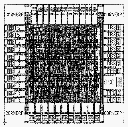
Fig. 1: Layout and technical data for the ENDOR-chip
To satisfy the growing demand for engineers trained in the design of integrated circuits (ICs), the Department of Electronics offers several academic courses to cover this topic. In order to establish fundamental knowledge on design flow, verification, and test of ICs, also some research projects are carried out at the Department. The main area in IC design is the wide topic of mixed signal ASICs in CMOS or BiCMOS technology. In the following chapters there will be an introduction to the facilities and the courses at the Department of Electronics. Furthermore some IC-projects of the year 1995 are presented.
A main part of the 1995 activity at the Department of Electronics in UNICHIP was training the students in the field of IC design. The Department offers five courses to cover the following topics:
In order to get a deeper understanding of the problems encountered with analogue integrated circuit design, two special courses at the EPFL in Lausanne/Switzerland were attended by members of the project team. The participation on some international conferences helps to establish good contact to the scientific community [3].
The AUSTROCHIP '95 Workshop in Graz was organized by the project team.
The following table shows the titles and some related information on all courses related to IC design offered at the Department of Electronics.
There were 10 diploma theses finished in 1995. Some of them where carried out in close cooperation with the three major enterprises in Austria dealing with IC design and manufacturing (AMS, Siemens-EZM and MIKRON).
title of the course          type  hours/term  participants/year

Integrierte Schaltungen 1     VO       30              80

Integrierte Schaltungen 2     VO       30              45

Integrierte Schaltungen 2     UE       30              45

Testen Integrierter           LU       45              36
Schaltungen

Elektronikprojekt             PR       90              10
We are using the following hardware components in our courses as well as for research projects:
We are using the following software-tools in our courses and for research projects:
In many courses there is a practical aspect that leads to some implementation and fabrication of chips by means of MPW (Multi-Project-Wafer) runs.
The I2C-bus is widely used in microcontroller applications. This student project was done by two persons. It started with schematic entry followed by simulation using MModels in LSim and ended with a standard-cell layout for a 1.2µm CMOS-process. This layout is part of the ELEVE-chip, which is currently on the way to fabrication.
In this project a transimpedance amplifier circuit of a given topology was brought from simulation to layout. The circuit will be part of the ELEVE-chip.
Two input amplifiers for piezoresistive sensors used for measurement of the velocity of sound in fluids were developed in this project. One was based on a mere use of MOS transistors. In the second circuit also bipolar-transistors were used. The layout was created by means of SDL (Schematic-Driven-Layout) using device generators. The circuits will be part of a test-chip in BiCMOS technology, which is intended to be in the factory in the middle of spring 1996.
An N-MOS and a P-MOS transistor were designed using various layout styles. The target was to reach an on-resistance of less than 10 ohms. Both transistors are part of the ELEVE-chip for evaluation on the workbench.
A 1kx8 static RAM was developed using a generator tool from Mentor Graphics. The layout was done for a 1.2 µm CMOS-process.
To be able to cancel charge-injection in analogue switches often so called dummy-switches are used. This project was done to simulate this effect and to do a layout to proof the obtained results. Three different switches were layouted and are part of the ELEVE-chip.
The projects of the latest test-chip (EXPLORER [1]) were evaluated. The results for the various designs were as we expected them to be. They match the results from simulation very well.
To minimize size and power consumption of a handheld, battery-powered density-meter an ASIC (ENDOR) was developed. It consists of some peripheral logic for a microcontroller and a unit for quantizing and coding in a charge-balance A/D-converter and a periodic signal. The microcontroller communicates via bus signals and registers with the ASIC.
process             1,2µm CMOS

transistor count    app. 8.000

area                2,5*2,5 mm2

time for            app. 6 months
development

package-type        PLCC-44

Fig. 1: Layout and technical data for the ENDOR-chip
To speed up the analogue ASIC design it is necessary to use Schematic Driven Layout to offer consistency and ease of modification. As the devices in analogue integrated circuits are not part of a library they have to be generated according to properties attached to the element in the schematic representation of the circuit. In this project the following device generators for a BiCMOS process of AMS and the design environment of Mentor Graphics were developed:
Figure 2 shows two layouts for transistors created by means of device-generators.

Fig. 2: Layout of an MOS- (left) and a bipolar-transistor (right)
In this project we had a close cooperation with AMS with the aim to incorporate these device-generators in the support-tool for customers.
In this project the building blocks (SC-integrator, sampled comparator, etc.) for high resolution A/D-converters will be developed using SC-technique. The project is not finished by now.
The design of integrated circuits from the idea to the chip is the main goal for the project reported. To train the students in this field there are some academic courses offered. Some student projects were realized on a test-chip to evaluate the simulation and the layout. There are also some research projects that are all together in the field of mixed-signal ASICs for sensor applications.
At the Department of Electronics there is a close cooperation to some firms mainly situated in Graz. Many students take the opportunity to do their thesis in one of them.
Although there are some contacts to small and medium sized enterprises the overall situation of technology transfer in the field of integrated circuit design is not as it should be.
The "Steiermärkische Landesregierung, Abteilung für Wirtschaftsförderung" is funding this project by carrying a main part of the costs for personnel. It would not be possible without this funding to have a continuous activity in the area of IC-design at the Department of Electronics.
[1] H. Senn et. al.: "Ein ASIC für die Ausbildung an integrierten Schaltungen", Grundlagen und Technologie elektronischer Bauelemente - Tagungsbericht, 1995, pp. 49 - 52.
[2] W. Meusburger, H. Senn, P. Söser: "Entwicklung von Device-Generatoren zur Unterstützung des Analog-IC-Designs mit Mentor V8", Austro-Chip '95 - Tagungsband, 1995, pp. 169 - 174.
[3] P. Söser: "Über die Entwicklung anwendungsspezifischer integrierter Schaltungen", Bericht der Herbsttagung der Studiengruppe für Elektronische Instrumentierung, 1995, pp. 8 - 14.
Univ.-Prof. Dr. Hans LEOPOLD
Institut für Elektronik, TU Graz, Graz, Austria
Last Name      First Name     Status              Remarks

Leopold        Hans           university
                              professor

Röhrer         Robert         associate
                              professor

Söser          Peter          assistant
                              professor

Meusburger     Walter         assistant
                              professor

Senn           Helmuth        research scientist  100% funded