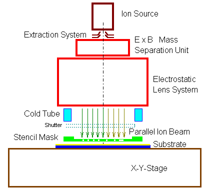
Fig. 1: Schematics of Masked Ion Beam Lithography (MIBL) stepper [1].
This project comprises three separate activities, each of which is partly related to the discontinued GMe focal-point activity on Ion Projection Lithography (IPL). The first activity made use of the GMe's ALPHA ion projector as an illumination unit for Masked Ion Beam Lithography (MIBL). The second activity involved experiments for the development of a three-level resist process that permits the indirect structuring of thick resist layers by ion beam exposure. Finally, the processes that are otherwise used for the preparation of field emitter displays were applied to the preparation of a micro-mechanical device, namely, of a dust collector for space experiments.
The ALPHA ion projector, which has been developed by the Viennese company IMS and has been bought by the GMe in the late eighties, has successfully been used in the past years to demonstrate the feasibility of Ion Projection Lithography (IPL). Due to wear and aging of crucial parts of this machine, a continued operation would have required considerable repairs and investments, and did therefore not appear feasible. Consequently, the GMe decided in 1995 to sell the ALPHA ion projector back to IMS, who were entitled in the agreement to dismantle the machine.
During the past years, the focus of the attention of IMS has shifted from demagnifying IPL to 1 : 1 Masked Ion Beam Lithography (MIBL) due to the greater simplicity of the required set-up. Currently, IMS is constructing a dedicated MIBL module (access to which will be available for the GMe under the selling agreement); for first MIBL experiments, the ALPHA ion projector was used as an illumination unit during the last months of its operation.
One of the key applications of MIBL will be the preparation of emitter tips for field emitter displays where sub-micrometer structures are required over a large area. All technological processes that permit to prepare those tips require relatively thick resist layers, into which structures with a high aspect ratio have to be transferred. The energy of an ion beam is not sufficient to expose these layers over their entire thickness; a multi-level process is therefore required for structure transfer.
With a similar technique, although with electron beam rather than ion beam exposure, special microstructured surfaces for an ESA space experiment were produced for the Austrian Research Center Seibersdorf. These surfaces will be used during the ROSETTA Mission to collect dust emitted from a comet; the dust particles will be imaged and classified by means of an atomic force microscope (AFM).
Optical and x-ray proximity printing systems are resolution limited by diffraction and beam dispersion. Parallel dispersion free ion beam systems are therefore ideal to transfer stencil mask patterns onto all sorts of non-ideal substrates. Figure 1 shows the schematics of a 1:1 MIBL system. Hydrogen or Helium ion beams are extracted from a suitable ion source and ExB mass separation unit. Using a proper electrostatic lens system, a parallel broad ion beam can be obtained. Ion beam induced mask heating effects can be compensated by radiation cooling using a cold tube that surrounds the mask exposure station. The virtual source size can be as small as 10 µm and, implementing proper electrostatic systems, the divergence of the ion beam illuminating a point in the stencil mask can be as low as 30 µrad. Thus, there is a penumbrial blur of only 30 nm for a gap of 1 mm between stencil mask and substrate.
Fig. 1: Schematics of Masked Ion Beam Lithography (MIBL) stepper [1].
A feasibility study was performed with the GMe' ALPHA ion projector operated in the MIBL (Masked Ion Beam Lithography) mode with 10x10 mm2 exposure field (Fig. 2).
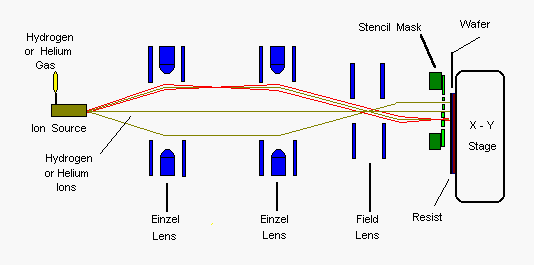
Fig. 2. ALPHA ion projector of the GMe as used in the MIBL mode [1].
Promising applications of the MIBL technique include the fabrication of flat panel displays based on vacuum electronics (field emitter displays), surface acoustic wave and micro-optic devices and - in combination with reactive ion etching - the fabrication of micro electro-mechanical systems (MEMS).
The goal of this investigation was the preparation of circularly shaped openings with a diameter of about 0.8 µm in OCG 6512 resist with a thickness of 1.2 µm. These structures are needed for the production of field emitter displays. The energy of the 55 keV H+ ion beam produced by the ALPHA ion projector was not sufficient to expose the resist over its entire thickness. Therefore, a three-level process had to be developed: A 30 nm thick titanium layer was evaporated on the 1.2 µm thick OCG 6512 resist spun on the substrate. The titanium layer was coated with 250 nm of ion sensitive resist AZ PF 514. The 55 keV H+ ions could fully expose this thin resist film through a galvanic over-grown Ni mask with openings down to 0.5 µm. After the exposure, the resist was wet chemically developed in undiluted AZ 518 developer. Next, the titanium layer was opened by microwave assisted reactive plasma etching with SF6. Finally, the bottom OCG 6512 resist was plasma etched in a mixture of oxygen and CF4. Both plasma etching processes were carried out in the Technics ECR 4000 RIE unit specially built for the TU Vienna. Figure 3 shows the relatively steep slopes in the bottom resist after the etching procedure. In order to assess the local etching rate within a hole, the etching was intentionally stopped before it reached the substrate.
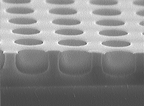
Fig. 3: Cross-section of the three-level resist after partial RIE etching of the OCG 6512.
For a space experiment, surfaces are required that can collect small dust particles (50 - 500 nm diameter) with high efficiency and without damage to the particles. These surfaces must convert the kinetic energy of the incoming dust particles by inelastic processes in order to avoid reflection of the particles. Free-standing columns of 0.3 µm diameter and 1.5 µm height were produced by means of electron beam lithography (Fig. 4). An impinging particle may break a number of these columns, thereby incurring an inelastic energy loss E per column:
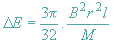
where B and M are fracture stress and modulus of the column material respectively; r and l are radius and length of the columns, respectively. The properties of these "collector surfaces" can be tailored to the particular requirements by variation of the column dimensions. By ion etching the structures of Fig. 4 into the Si substrate material it was possible to produce arrays of free-standing cones whose fracture energy is considerably lower than that of the resist columns.
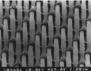
Fig. 4: Micro-columns in resist material.
This work was supported in part by the Austrian East-West-Project (OWP-92 GZ 45.291/I-IV/6a/93).
[1] E. Hammel, H. Löschner, G. Stengl, H. Buschbeck, A. Chalupka, H. Vonach, E. Cekan, W. Fallmann, G. Paschke, G. Stangl: "Masked Ion Beam Lithography for Proximity Printing", Microelectronic Engineering 30 (1996), 241 - 244.
Univ-Prof. Dr. Wolfgang FALLMANN
Institut für Allgemeine Elektrotechnik und Elektronik, TU Wien.
Last Name      First Name     Status              Remarks

Cekan          Ewald          dissertation        partial GMe funding

Fallmann       Wolfgang       university
                              professor

Riedling       Karl           associate
                              professor

Schalko        Johannes       dissertation        partial GMe funding

Stangl         Günther        technician