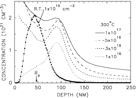
Fig. 1: SIMS potassium profiles for C60 films implanted with 30 keV K+ at room temperature (1x10¹⁶) and at 300 °C (1, 3, 5 and 10x1016 cm-2).
This paper demonstrates applications of surface analysis techniques for the investigation and characterization of materials and production processes. SIMS depth profile measurements of implanted erbium in silicon demonstrate that high precision measurements of low concentrations are necessary to assist implantation and simulation groups. Measurements of potassium profiles in fullerene films were done to investigate diffusion processes in order to optimize material properties.
Surface analysis techniques play an important role for supporting material development and process optimization. One of the most common techniques is the Secondary Ion Mass Spectrometry (SIMS). This is due to the high detection power of the method, the fact that all elements are detectable and the possibility of registering two- and three-dimensional distributions of trace elements.
To support various investigations in the field of microelectronics, the performance of analytical methods has to be increased. The actual questions of the technology demand a permanent development of the precision of measurements, especially at very low concentrations. The supervision of the implantation process stability by measurements of depth profiles for erbium demonstrates the support of optimizing production processes. Investigation of the implanted potassium distribution in C60 fullerenes supplies information for the development of new materials.
The ion implantation of 2 MV erbium in silicon was performed at room temperature with doses of 3,13 x10¹³ and 8,13x1013 cm-2. To determine the diffusion coefficient of erbium in silicon, one series of the samples was tempered at 900° C for 30 min in nitrogen.
The films of chromatographically purified C60 were prepared on silicon substrates by vacuum deposition. Ion implantation of 30 keV 39K+ was performed at 300 °C in a vacuum better than 10-4 Pa. The depth profiles were measured using 5.5 keV O2+ primary ions.
The SIMS depth profiles of implanted erbium in silicon show no broadening of the erbium implantation profiles during the temperature treatment. The maximum concentration of erbium was about 2x10¹⁸ atoms per cm3, the profiles were Gaussian like. The detection limit was lower than 1x10¹⁵ atoms per cm3. This indicates that there is no significant diffusion of erbium at a temperature of 900° C.
Figure 1 shows the depth profile of 39K+ for samples implanted with 30 keV K0 at room temperature (1x1016 cm-2) and at 300 °C (1, 3, 5 and 10x1016 cm-2). For room temperature implantation, the experimental profile is Gaussian-like with a weak diffusion induced tail at greater depths. At 300 °C implantation temperature a peak appears in the tail region at about 100 nm, and the K-concentration within the theoretical ion range is strongly reduced. An increase of the dose leads to a subsequent increase of the peak at about 100 nm and to a slight shift of its maximum into the depth. However, with increasing dose the K concentration in this region tends to saturate at a value of about 2x1021 cm-3. A certain amount of K diffuses out to the surface, but the diffusion into the depth is more pronounced. In all samples more than 70% of the implanted atoms are found underneath a 70 nm surface layer. Raman spectra indicate that there is a passivating a-C surface layer and the accumulation of K is at the a-C/C60 interface. These structures may have useful applications for the new Tc superconducting devices on the basis of fullerenes which can be handled on air [1, 2].
Fig. 1: SIMS potassium profiles for C60 films implanted with 30 keV K+ at room temperature (1x10¹⁶) and at 300 °C (1, 3, 5 and 10x1016 cm-2).
[1] J. Kastner, H. Kuzmany, L. Palmetshofer, K. Piplits: "Formation of air stable buried K-fulleride layers by ion implantation", Synthetic Metals 70 (1995) 1469 - 1470.
[2] L. Palmetshofer, M. Geretschläger, J. Kastner, H. Kutzmany, K. Piplits: "Characterization of K-fulleride layers formed by ion implantation", J. Appl. Phys. 77 (3), 1995.
Dr. Herbert HUTTER, Univ.-Prof. Dr. Manfred GRASSERBAUER
Institute of Analytical Chemistry, Vienna University of Technology, Vienna, Austria
Last Name      First Name     Status              Remarks

Grasserbauer   Manfred        university
                              professor

Hutter         Herbert        assistant
                              professor

Piplits        Kurt           technican

Brunner        Christian      dissertation