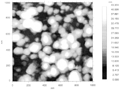
Fig. 1: Contact-AFM image of the as-grown layer
The surface topography and structure of low-pressure chemical vapor deposited silicon films on thermal oxide grown on (100)-silicon substrates have been investigated on a nanometer scale by scanning force microscopy, tunneling barrier height imaging (TBI) and constant current scanning tunneling microscopy (STM). As a result we have found that surface topography and roughness are mainly determined by the deposition process. Films deposited at 620°C show a columnar structure represented by hillocks with lateral dimensions between 50 and 150 nm and surface roughness between 7 and 14 nm. Doping by high temperature diffusion and subsequent annealing causes a complete recrystallization of the film, leading to lateral grain sizes between 200 and 600 nm.
Thin films of polycrystalline silicon prepared by chemical vapor deposition (CVD) are used in different applications in today's integrated circuit device technology. In addition to its use as gate electrodes of metal-oxide-semiconductor (MOS) devices and interconnections in VLSI circuits, polysilicon is being used as high-value load resistor in static RAMs, floating gates in electrically alterable ROMs (EEPROMs) and transistor emitters in bipolar technology.
Atomic force microscopy (AFM) and scanning tunneling microscopy are powerful tools for real-space surface imaging with high 3D resolution. Atomic resolution of surface structures can be achieved in a variety of fields such as biology, electrochemistry, and semiconductor materials. Additional information about electrical properties of conducting materials can be obtained in applying STM-related modulation techniques as differential conductance measurements and tunneling barrier height imaging (TBI). TBI in the case of semiconductors is very sensitive to local dopant variation induced changes of the band structure.
In the present work we report on structure and surface roughness investigations of polysilicon produced by LPCVD followed by high temperature diffusion doping, performed by contact AFM and STM measurements under ambient and high vacuum conditions. The samples have been taken from production-line test wafers, produced by high-volume equipment.
The measurements have been performed using a commercial UHV AFM/STM, with a 5 µm range tube-scanner driving the sample. Scanner calibration at atomic resolution has been performed by the manufacturer and proved by the authors for higher scan ranges using flat lithographic gratings.
The STM measurements have been performed using electrochemically etched PtIr tips with a 15° interior angle and a 50 nm radius of curvature. Commercially available silicon nitride cantilevers characterized by a 35° interior angle and 20 nm radius of curvature have been used for the contact-AFM measurements. Force calibration for individual cantilevers has been obtained by measuring force-distance curves.
The polycrystalline layers have been deposited by thermal decomposition of undiluted silane in a high-volume production LPCVD reactor at 620 °C onto (100) n-type silicon wafers covered with 100 nm of thermally grown silicon dioxide. Deposition at this temperature is known to produce a well-defined columnar structure that allows easy dopant diffusion along the grain boundaries and therefore is selected for intermediately doped layers in MOS gate electrode and interconnect applications. Ex-situ phosphorus doping has been applied to some of the wafers by gaseous predeposition using a POCl3 source at 970 °C (sheet resistance 10 W/square) and 900 °C (15 W/square), followed by deglazing in buffered oxide etch (BOE). Additional selective silicon oxide etching has been applied by dipping the samples in 40% HF acid for 30 seconds.
The low conductivity of the as-grown layer has restricted our measurements to contact-AFM. Images of the film deposited at 620 °C exhibit a fine polycrystalline structure (Fig. 1) typical for LPCVD films deposited above the amorphous-polycrystalline transition temperature [1]. The lateral dimension of the columnar crystallites represented by the bright regions of the topograph in Fig. 1 varies between 50 and 150 nm. Corrugation and surface roughness are determined by height differences of the individual crystallites and depend on the selected position on the sample. The films show a significant increase of an order of magnitude in surface roughness compared to the substrate and layers deposited under amorphous growth conditions.
Fig. 1: Contact-AFM image of the as-grown layer
The contact-AFM picture of a layer phosphorus doped at 900 °C shows hillocks comparable in size and shape to the as-grown film in Fig. 1, but no evidence for larger size structures one might expect from the recrystallization caused by the high-temperature doping procedure. In Fig. 2, the topographic data have been numerically differentiated with respect to the lateral coordinates to enhance short-scale corrugation and have been convoluted with the topographic data. This synthetic image results in a contrast enhancement of grain boundaries and makes a well-defined lateral equiaxed structure observable. Typical lateral dimensions of the grains are 200 nm, but ranging up to 400 nm. In layers phosphorus doped at 970°C the differentiated topograph reveals larger grain sizes up to about 600 nm.
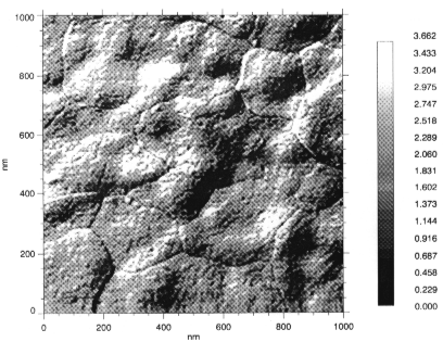
Fig. 2: Differentiated and convoluted contact-AFM image of a doped layer, showing grain boundaries
All the measurements have been performed by contact AFM using the same silicon nitride tip. At least 20 images of 1x1 µm2 have been acquired on several positions. Areas have been chosen randomly on each sample. Roughness values have been calculated from each image using standard software which fits a plane to the entire image, determines the deviation of each image point from this plane and calculates the arithmetic roughness Ra and root-mean-square Rrms. The values of the roughness are largest in the as-grown layers (Rrms= 13.7 nm), smaller in those doped at 970°C (8.6 nm) and 900°C (7.5 nm).
The scanning probe techniques applied in this work have proven to be superior to other techniques for surface topography and roughness determinations. It has been shown that both are essentially determined by the deposition process. Large grains anticipated to occur during the doping process at 900 - 970 °C, clearly become observable by differentiating and convoluting contact-AFM topographic data.
The authors wish to thank Dr. M. Pippan and Dr. H. Noll of Austria Mikro Systeme International for kindly supplying us with the sample-wafers.
[1] T.I. Kamins, M.M. Mandurah and K.C. Saraswat: "Structure and stability of low pressure chemically vapour-deposited silicon films", J. Electrochem. Soc. 125, 1979, pp. 927 - 932.
Univ.-Prof. Dr. F. KUCHAR
Institute of Physics, University of Leoben
Last Name      First Name     Status              Remarks

Kuchar         F.             university
                              professor

McCombe        B.D.           university          5% GMe
                              professor

Lutz           J.             assistant
                              professor

Kulac          I.             dissertation        100% GMe

Pirker         H.             technician          10% GMe

Pleschinger    A.             dissertation