Growth, Doping and Structuring of Si/SiGe/SiC
G. Brunthaler, A. Darhuber, T. Grill, Ch. Penn, F.Schäffler, J.Stangl, G. Steinbacher, H. Straub, S.Zerlauth, Y. Zhuang, G. Bauer
Institut für Halbleiterphysik, Johannes Kepler Universität,
A-4040 Linz, Austria
We report on the structural and optical properties of silicon-based heterostructures containing ternary Si1-x-yGexCy alloys. Both single and multiple quantum wells were grown by molecular beam epitaxy and their quality was assessed by x-ray rocking analyses and by photoluminescence (PL) measurements. Optimum growth temperatures with respect to carbon incorporation and layer quality were found to be at around 500 °C. We observed well behaved PL signals from Si1-yCy single layers and Si/Si1-yCy multiple quantum wells as well as from Si/Si1-yCy/Si1-xGex superlattices with carbon concentrations up to 1.7%. For an investigation of the thermal stability of these intrinsically metastable layers, ex-situ annealing experiments were conducted in the temperature range between 500 °C and 900 °C. Up to about 725 °C an improvement of the PL signals both with respect to intensity and linewidth is observed, whereas the amount of substitutional carbon remained unaffected. After annealing at 725 °C we observed the narrowest linewidth in a Si1-yCy single layer reported so far in the literature. At higher annealing temperatures the PL signal decreases, but it takes more than 850 °C to observe a decrease of the substitutional carbon concentration in x-ray measurements. The results indicate that carbon containing epi-layers of high crystal quality can be grown by MBE, and that thermal stability is good enough to make the material interesting for device applications.
Si1-x-y GexCy Layers: Growth and Characterization
(F. Schäffler, S. Zerlauth, Ch. Penn)
It is the outstanding property of Si-based heterostructures to provide the application relevant combination of band structure engineering and silicon very-large-scale-integration (VLSI) compatibility. In the past few years most of the basic properties regarding the lattice mismatched Si/Si1-xGex material combination, and especially the effects of strain on the band offsets and bandgaps, have been investigated. It has been found that the band offset at the interface between a pseudomorphic Si1-xGex layer and a Si substrate occurs almost exclusively in the valence bands, whereas a tensilely strained Si layer is required for the implementation of useful conduction band offsets. By employing proper combinations of pseudomorphic and strain-relaxed epi-layers, both tensile and compressive strains can be custom designed, without sacrificing the important advantages of a Si substrate and the basic compatibility with Si technologies.
By exploiting strain-engineering as an additional degree of freedom, a wide variety of devices structures have been implemented in the Si/Si1-xGex material system, reaching from heterobipolar transistors (HBT) over p- and n-type modulation-doped field effect transistors (MODFET) to optical detectors in the near infrared, and even light emitters. Nevertheless, so far only the pseudomorphic Si/SiGe HBT has reached production status, whereas other devices with demonstrated superior properties, such as the n-type MODFET, are still restricted to test devices on a laboratory level. The main reason for the much slower development of the MODFET lies in the necessity for strain relaxed
Si1-xGex buffer layers. These have successfully been implemented by several research groups, but defect and morphology control still require further refinement to make them suited for a production environment.
Ternary Si1-x-yGexCy alloys offer an alternative route to strain-engineering in silicon-based heterostructures, which finally may overcome the problems imposed by relaxed buffer layers: Due to the covalent radii of C and Ge, which are smaller, and larger than that of Si, respectively, both compressively and tensilely strained, pseudomorphic layers can be implemented by proper adjustment of x and y in the active layers of a heterostructure. However, in contrast to the binary Si1-xGex alloys, which are thermodynamically stable for all compositions x, carbon has almost negligible solid solubility in both Si and Ge, but, on the other hand, tends to the formation of stoichiometric SiC. Since strain engineering requires C concentrations of a few percent to provide useful modifications of the band structure, non-equilibrium growth conditions at sufficiently low temperatures have to be established. This requires an optimization of the growth parameters to allow sufficiently high C incorporation without excessive degradation of the crystal quality through the undesirable generation of point defects. Also, the surface morphology has to be controlled in order to suppress strain-induced three-dimensional growth. In the following we report on the progress that has been made in Linz regarding the growth of heterostructures containing ternary Si1-x-yGexCy alloys. The main emphasis in 1996 has been put on the structural and optical qualities of these layer sequences, which are an essential prerequisite for any further assessment of the future role Si1-x-yGexCy alloys can play in the field of application-driven band structure engineering.
Sample Preparation and Characterization
The ternary Si1-x-yGexCy alloys were grown in a newly commissioned RIBER SIVA 45 MBE machine equipped with electron beam evaporators for Si, Ge, and C, and dopant effusion cells for Sb (n-type) and B (p-type). High-purity, single crystalline ingots are used for the Si and Ge sources, whereas pyrolytic graphite is used in the carbon evaporator. The fluxes of all three matrix materials are monitored, and feedback-controlled, by a quadrupole mass spectrometer with a cross-beam ion source and PID controllers. The mass spectrometer signals are calibrated by epitaxial growth of Si1-xGex and Si1-yCy reference layers, the compositions and layer thicknesses of which are determined by x-ray rocking analyses in combination with dynamic simulations. The flux stability, especially of the C source, which is the most critical one because of the small fluxes required, is occasionally checked by quantitative SIMS analysis.
High-resistivity (FZ, r > 1000 Wcm) Si substrates of 100 mm diameter are chemically precleaned either by oxide removal in 5% HF or by a standard RCA cleaning procedure. Immediately after precleaning the wafers are mounted in 125 mm diameter, all-silicon adapters, a total of six of which can be introduced into the magazine of the load-lock chamber. After pump-down of the load-lock chamber into the 10-9 mbar range, the wafers are transferred into the growth chamber, where they are suspended by Mo-clamps underneath a radiative substrate heater made of pyrolytic graphite (PG). Prior to growth, which always commences with a Si buffer layer of 100 to 200 nm thickness, a thermal cleaning step is performed at 900 °C for typically 5 min to remove SiO2 and possible organic contaminations from the surface. This step can be controlled by in-situ reflection high energy electron diffraction (RHEED), which reveals a (2x1) reconstruction of the bare Si surface as soon as the amorphous oxide has been flashed off.
The heterostructures are routinely characterized by x-ray diffraction, which yields, as mentioned, in the case of single layers composition and layer thickness. In the case of multiple quantum wells and superlattices, the period length is the primary information derived from rocking measurements. The compositions and the thicknesses of the individual layers can also be extracted by fitting of dynamic simulation curves, however, a certain degree of ambiguity remains. For that reason additional information is useful, such as the composition determined by SIMS analysis, or Rutherford backscattering (RBS). The latter technique is not directly applicable to C, because of the minor backscattering yield from the light elements. Therefore, we are presently trying in collaboration with the University of Padua, to exploit a nuclear resonance with broad enough scattering cross section to enhance the back scattering yield to an extent that allows for an absolute, depth resolved evaluation of the carbon content.
For an investigation of the thermal stability of the strained Si1-yCy layers annealing at temperatures between 500°C and 900°C was performed under vacuum either in a furnace or directly in the MBE growth chamber.
Photoluminescence (PL) spectroscopy is a versatile technique, which not only provides information on the band gaps and the band offsets, but is also a sensitive indicator of the overall crystal quality of the layers. This is of special interest for an optimization of the low temperature growth conditions required for the metastable incorporation of carbon, because the PL signal is strongly suppressed, once the density of growth-induced non-radiative recombination centers becomes too high. For our investigations, PL was excited by the 488 nm line of an Ar+ laser, analyzed in a 0.32 m grating spectrometer and detected by a North Coast Ge detector in a standard lock-in technique. A temperature-variable He cryostat allowed for temperature dependent measurements in the range between 1.6 and 300 K.
Experimental Results
Three types of samples were grown for these studies, namely Si1-yCy single layers,
Si/Si1-yCy multiple quantum wells, and strain compensated Si/Si1-yCy/Si1-xGex superlattices. In the first two types of samples the band offset is almost exclusively restricted to the conduction band, which is energetically lower in the tensilely strained Si1-yCy layers due to a strain splitting of the six-fold degenerate, Si-like conduction band. The situation is analogous to strained Si grown on a relaxed Si1-xGex buffer layer and is therefore of special interest for the implementation of n-type MODFETs. Band alignment in the Si/Si1-yCy/Si1-xGex superlattices, which are interesting for infrared detector applications because of the inherent strain compensation, is more complex: Since the Si1-xGex layers introduce an additional valence band offset, carrier confinement is indirect both in k-space and in real space, with electrons being located in the Si1-yCy layers and holes in the Si1-xGex layers.
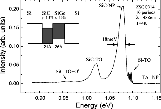
At growth temperatures of around 500 °C the as-grown samples of all three types showed well behaved PL signals. There is presently only one other group worldwide that has published comparable PL spectra from MBE-grown layers. As an example, Fig. 1 shows the spectrum of a ten-period Si/Si0.989C0.011/Si0.9Ge0.1 superlattice together with a schematic view of the strain-induced band alignment. Two distinct peaks are observed, which originate from band edge recombination in the vicinity of the Si1-yCy/Si1-xGex interface, where the wave functions of electrons and holes have finite overlap. The peak at higher energies, labeled SiC-NP, results from the no-phonon transition, whereas the other peak is its TO phonon replica. A NP transition in an indirect gap material is only possible if symmetry breaking mechanisms are present, such as the presence of a heterointerfaces and/or the statistical fluctuations in a random alloy, which is both the case in our layers. The relative strength of the superlattice related peaks can by judged by comparison with the TO replicas originating from the Si layers and from the substrate. Obviously, the quantum wells very efficiently collect electron-hole pairs from the several µm deep excitation volume, and also maintain long enough lifetimes to allow the observation of radiative recombination. The strength of the bandgap PL signal is therefore an important indicator of the crystal quality, since an excessive amount of defects in the layers and at the heterointerfaces associated with non-radiative recombination would quench the PL signal altogether. This is indeed the case, when growth temperatures below 450°C are employed.
Fig. 1: PL spectrum of a ten-period Si/Si0.989C0.011/Si0.9Ge0.1 superlattice. The dominating signals are the no-phonon (NP) band edge recombination from the quantum well section and its TO-phonon replica. The shaded part of the spectrum results from the Si layers and the Si substrate.
Compared to the well established quantum well luminescence from single Si1-xGex layers, the PL signal in Fig. 1 is almost a factor of six broader. Since close to a factor of ten higher Ge concentrations are required to induce the same amount of strain that is provided by a given carbon concentration, the statistical fluctuations of both the well width and the well depth are much more pronounced in the case of a Si1-yCy layer of comparable average strain. In addition possible composition fluctuations from layer to layer may contribute to the line width from a superlattice. For the investigation of annealing effects we therefore mainly concentrated on single Si1-yCy layers, which were grown thin enough to remain with the critical thickness limitations, but thick enough to suppress quantum confinement effects. Save for the exciton binding energy, this way the true band gap recombination is measured without any necessity for the correction of confinement energies. In addition, cross checks with the multiple quantum well samples confirmed that the annealing behavior is qualitatively the same.
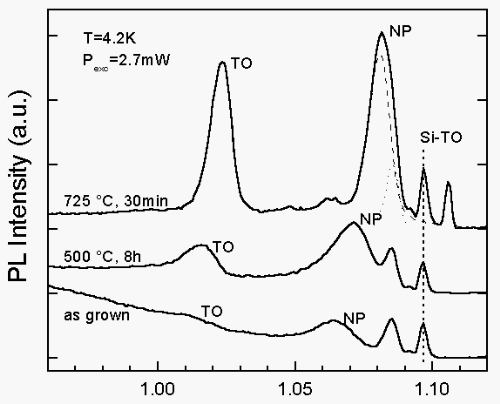
Fig. 2: Evolution of the PL signal of a single Si1-yCy layer for increasing annealing temperatures. Note the blue shift and the line narrowing.
Figure 2 shows a series of PL measurements from a 100 nm thick Si0.989C0.011 layer, which underwent annealing at successively higher temperatures in the range between 500 and 725 °C. There are three main effects associated with annealing: (i) The intensity of the band gap PL signal increases significantly within the range of annealing temperatures shown here. (ii) There is a noticeable blue shift of the PL lines amounting to about 15 meV. (iii) The line width after background subtraction becomes much narrower as the annealing temperature is increased. In fact, the linewidth of 8.4 meV in the topmost curve of Fig. 2 is the narrowest observed to date in a Si1-yCy layer.
Most interesting, the pronounced changes of the PL signal are not associated with a change of the substitutional carbon concentration, as has been checked by x-ray rocking analyses. Only at higher annealing temperatures of >850 °C a loss of substitutional carbon is observed, whereas the PL intensity starts decaying already at about 750 °C.
Since changes of the average C concentration can be ruled out, and quantum confinement effects through possible short range diffusion of substitutional carbon can be neglected in the thick layers used here, the development of the PL signal has to have other reasons. To further elucidate these mechanisms, PL measurements of the samples with the highest PL intensity were recorded as a function of the measurement temperature. This is shown in Fig. 3, where the TO-replica of the band gap recombination, which is not affected by spurious signals from the Si substrate, is plotted for measurement temperatures in the range between 4.2 and 20 K. The most striking feature of these measurements, which was confirmed by experiments on the quantum well samples, is a red shift concomitant with a decay of the intensity as the temperature is increased.
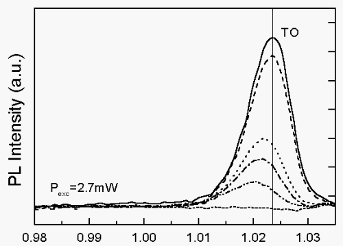
Fig. 3: Red shift of the PL signal with increasing measurement temperature. The TO-phonon replica is plotted here, because it is free of substrate-related signals.
Discussion
A consistent interpretation of the annealing effects and of the red shift with higher measurement temperature can be derived, when assuming that the as-grown samples contain non-radiative recombination centers as well as non-statistical fluctuations of the local, substitutional carbon concentration. The latter may be associated with C2 and C3 molecules, which are observed in the mass spectrum of the carbon molecular beam, and which are tentatively not completely dissociated at the low growth temperatures employed. Based on these assumptions the following effects will occur during annealing:
(i) At low annealing temperatures (middle curve in Fig. 2, 500 °C for 8 h), non-radiative recombination centers associated with growth defects begin to disappear. This leads to an increase of the PL intensity, but only to a minor decrease of the line width.
(ii) At higher annealing temperatures (upper curve in Fig. 2, 725 °C, 30 min) a redistribution of carbon on a local scale occurs, which leads to the dissolution of local carbon accumulations, introduced e.g. by molecular forms of evaporated C. The overall effect is a more homogeneous, statistical distribution of carbon, which causes two effects: First, the PL signal experiences a blue shift, because homogenization of the carbon concentration smears out the local band gap minima in regions of originally enhanced concentration. Second, the line width becomes narrower as the statistical fluctuations become smaller. This interpretation is corroborated by the fact that the ratio between NP signal and TO-replica decreases, which means a reduction of the symmetry-breaking alloy fluctuations.
(iii) Although the fluctuations of the carbon concentration become more homogeneous upon annealing, the remaining alloy is still random. This explains the red shift with increasing measurement temperature, which results from carriers bound to alloy fluctuations, as has been observed in Si1.xGex, too. With increasing temperature the electrons become mobile and establish an equilibrium distribution that preferentially fills the regions with the smallest band gaps.
(iv) The layers are thermally stable to beyond 850 °C, with no indications for a change of the average concentration of substitutional carbon. Thus noticeable diffusion of carbon or SiC precipitation requires higher temperatures and should not be a severe limitation for device processing.
Conclusions and Outlook
We have established MBE growth conditions for high-quality Si/Si1-yCy and Si/Si1-yCy/ Si1-xGex samples with substitutional carbon concentrations of up to 1.7%. Well-behaved PL signals from band edge recombination in the Si1-yCy layers, and at the Si1-yCy/ Si1-xGex interface, respectively, have been observed. The quality of the layers improves significantly upon annealing at moderate temperatures of about 725 °C, without affecting the substitutional carbon concentration. At these temperatures annealing mainly reduces the defect density in the layers and leads to a more homogeneous distribution of substitutional carbon. The layers are thermally stable to beyond 850 °C, where we observe first indications for a reduction of the substitutional carbon content.
Successful growth of carbon-containing, Si-based heterostructures is an important prerequisite for a future implementation of n-type MODFETs with tensilely strained Si1-yCy quantum wells. In a next step growth conditions have to be adjusted to allow somewhat higher carbon concentrations of about 2 – 2.5%, which are necessary for the required conduction band offset of 130 to 160 meV. Such layers will allow the fabrication of MODFETs for an assessment of the electronic properties.
Nanostructuring of Semiconductors
(G. Brunthaler, H. Straub, A. Darhuber, T. Grill, Y. Zhuang, G. Bauer)
Introduction
The realization of semiconductor nanostructures is relevant for future electronic devices, optical emitters and the investigation of basic physical properties. In II-VI semiconductors the realization of wide band-gap blue-green diode lasers [13], [14] initiated the interest in light emitters from nanostructures. In such a nanostructure it is expected that low threshold laser structures can be realized.
In Si/SiGe heterostructures the investigation of nanostructures is driven by the miniaturization of today’s integrated circuits and the potential of the Si/SiGe material system to increase the performance of such devices. Both material systems mentioned consist of strained layers and the investigation of strain relaxation effects due to the formation of laterally patterned nanostructures is needed for practical implementations.
The purpose of our Si/SiGe study was to find a reliable etching procedure for the fabrication of Si/SiGe sub-micron structures. There are previous reports in the literature that in particular the sidewall steepness of SiGe embedded in Si is much worse than that of silicon. The etched Si/SiGe structures were than structurally characterized by x-ray diffraction.
Sample Preparation
The II-VI and Si/SiGe heterostructures were both grown by molecular beam epitaxy in Linz. The CdZnSe/ZnSe single quantum well (QW) heterostructures consist of a 1.1 µm thick, fully relaxed ZnSe buffer on top of the GaAs (001) substrate (grown by W. Faschinger). A 10 nm CdZnSe layer forms the QW and a 100 nm ZnSe layer acts as a cap. High density periodic patterns were defined either by holographic or electron beam lithography. In the case of e-beam lithography, well defined arrays of 40 x 40 µm2 with wires and dots of different lateral size were written into a 150 nm thick polymethylmethacrylate (PMMA) resist layer. The lateral distance between individual pattern arrays is 150 µm. After deposition of a 40 nm thick titanium layer, a lift of process was used to produce the metallic structures on top of the sample with area filling factors between 0.5 and 0.15. These patterns were transferred into the QW structure by reactive ion etching (RIE).
During the RIE process the sample is exposed to a reactive gas plasma which contains active species that etch the material by chemical reactions. A CH4/H2 gas mixture (1:6 volume ratio) with a high frequency power of 90 W (corresponding to a DC bias of 450 V) at a pressure of 3.3 Pa (25 mTorr) is used for the II-VI compounds. The surface morphology and the lateral sizes of the etched structures were investigated by scanning electron microscopy (SEM). A typical SEM micrograph for small wires is shown in Fig. 4.
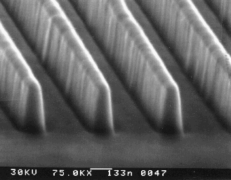
Fig. 4: Scanning electron microscopy image of CdZnSe/ZnSe wire structures defined by electron beam lithography and fabricated by reactive ion etching with a CH4/H2 gas mixture.
Si substrates and Si/SiGe multiquantum well layers (Ge-content: about 20%, 10 periods, Si layer width: 20.5 nm, and SiGe layer width of 1.8 nm) were laterally patterned using holographic lithography (l = 458 nm) by reactive ion etching. The period of the wires is about 400 nm, the wire width about 200 nm. The etching depth is about 200 nm. The etching gases consisted of a mixture of SF6 and CH4 (90%/10% mixing ratio) using the following parameters. The rf-power was 30 Watt, the pressure 40 mTorr, the flowrate of SF6 was 50 sccm, and for CH4 it was about 2.5 sccm. (The corresponding parameters for the Si/SiGe MQW samples were the same). The remaining photoresist was taken off by an oxygen plasma. The surface morphology of the samples was investigated by scanning electron microscopy. The structural parameters were studied by different x-ray diffraction techniques, as described below.
Optical Investigations
Low temperature (T = 1.9 K) PL measurements were performed with an x-y mapping set-up with a spatial resolution of 30 µm (determined by the laser spot diameter). The Cd0.2Zn0.8Se QW embedded in ZnSe barriers (with a low temperature band gap Eg = 2.820 eV) was resonantly excited with an Ar+ ion laser at an energy of 2.708 eV (457.9 nm) with about 100 W/cm2. The PL spectra of the Cd0.2Zn0.8Se/ZnSe wires and dots with lateral dimensions between 80 and 1000 nm are shown in Fig. 5. The width of the PL emission line from the 2D reference mesa on the same sample is about 8 meV, a value which is essentially caused by alloy fluctuations in the ternary CdZnSe layer. Thus the splitting between free and bound excitons cannot be resolved.
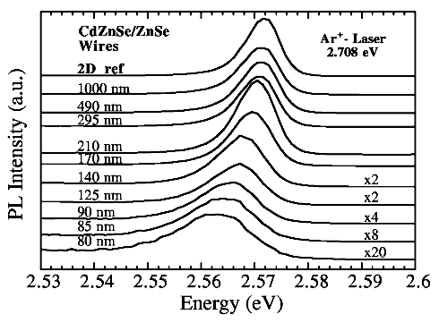
Fig. 5: Photoluminescence spectra of CdZnSe/ZnSe wire structures for lateral width of 80 to 1000 nm at 1.9 K. In addition the 2D quantum well reference spectrum on the same sample piece is shown.
Figure 6 shows the peak position of the PL line for wire and dot structures with lateral width between 80 and 1000 nm. A significant red shift occurs for wire sizes below 300 nm and dot sizes below 500 nm which is about 8 to 10 meV for the smallest wires and dots, respectively. The observed red shift will be discussed and compared with calculated band gap changes due to strain relaxation below.
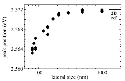
Fig. 6: Photoluminescence peak position of wire structures between 80 and 1000 nm for a resonant excitation energy of 2.708 eV (457.9 nm).
Strain Relaxation and Band-Gap Changes
Due to the formation of free perpendicular surfaces during the lateral patterning, the strained layers are able to relax partly. This is shown in Fig. 7 schematically for a thin wire structure. In order to calculate the detailed strain distribution of the wire structures, we follow an analytical method outlined by Faux and Haigh [15] but adopted it for our [110] oriented wires. This method solves the Airy stress equation by a Fourier series ansatz. The advantage of this method is that it is analytic, the disadvantage (as compared e.g. to finite element methods) is that only simple geometries can be treated with a restricted range of boundary conditions.
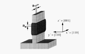
Fig. 7: Schematic strain relaxation of a laterally thin, partly relaxed CdZnSe/ZnSe wire.
Figure 8 shows the calculated strain distribution ey’y’, for a 80 nm wide wire of our CdZnSe/ZnSe structure, where the coordinate y´ in the epitaxial plane but perpendicular to the wires. The magnified displacements (by a factor 20) characterized by ey’y’ and ezz are shown in Fig. 9 for the wire cross section (the y´z-plane). It is clearly visible that the distortions are largest at the free surfaces. The shear component ey’z, which characterizes the deviations from a rectangular grid, is largest at the interface between the CdZnSe well and ZnSe barrier layers close to the free surface.
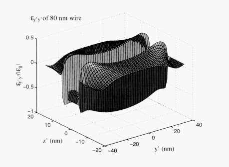
Fig. 8: Strain component ey’y’ for the wire cross section y´z with the y´ direction in the quantum well plane but perpendicular to the wire and the z direction along the growth direction.
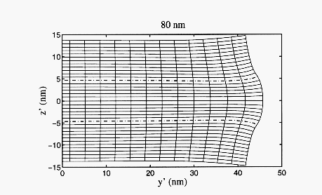
Fig. 9: The displacement, magnified by a factor 20, according to the strain components ey’y’ and ezz for the wire cross section (y´z-plane).
In <110> wires the non-uniform lattice deformation induces a piezoelectric polarization field [16], [17], [20]. The piezoelectric effect is directly connected with the shear components (shear strains ejk, j ¹ k) as these describe the distortions of the cubic crystallographic cell. The potential distribution due to the piezoelectric were calculated accordingly for our wire structure with a width of 80 nm. The potential difference between upper and lower interface along the z-direction is about 12 meV. This bending of the quantum well potential and the associated electric field leads to a Stark effect which shifts the energy levels in the center of the well only by about 0.5 meV. Compared to the observed red shifts and the changes of the band gap due to deformation potential coupling, the effects due to piezoelectric coupling will be only important at still smaller wire structures.
Due to the lateral wire confinement by RIE patterning in 80 nm structures, the eigenstate energies inside the CdZnSe well change by less than 0.5 meV for electrons and 0.4 meV for heavy holes. These additional lateral confinement energies (blue shifts) are much smaller than the experimentally observed red shifts and will not give a relevant contribution.
The band gap changes due to the elastic strain relaxation in the wire structures are much more important. For the conduction band, the strain induced energetic shifts are easily calculated as no splitting of degeneracies due to a tetragonal or orthorhombic distortion of the lattice occurs. Only the hydrostatic component of the lattice affects the position of the CB edge [18]. The situation for the VB is more complicated as even in the 2D QW system (tetragonal distortion without the presence of shear strain components), the four-fold degeneracy (G8, including spin) of the cubic Td crystal symmetry is removed. The energy levels of the valence band for cubic systems can be described by the k×p perturbation approach [19]. The effects of strain, confinement or other distortions can be included in the Hamiltonian of the system by using perturbation theory [22]. The deformation potential parameters av, b and d as introduced by Bir and Pikus [21] describe the energetic changes due to hydrostatic, tetragonal and shear deformations of the lattice, respectively. The solutions for the 6x6 Hamiltonian are obtained by numerical diagonalization for a given set of strain components which itself depends on the y´-z position inside the wire cross section. The resulting variation of the band gap over the cross section of the 80 nm wire is shown in Fig. 10.
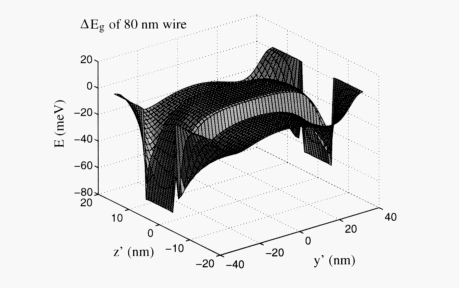
Fig. 10: Variation of the band-gap on the wire cross section (y´z-plane) for lateral wire width of 80 nm.
The calculated band gap changes of about 8 meV for the 80 nm wire structure are comparable with the experimentally observed PL line width of the 2D reference area on the sample. It is thus not expected to resolve any splitting of lines, but just a broadening and shift. It is also unknown how the PL emission efficiency is correlated with the spatial position in the wire structure. This efficiency depends on the RIE induced damage near the free surfaces as well as on the carrier diffusion after generation by incident laser beam. In Fig. 11 the calculated averaged energetic band gap shift is compared with the experimentally observed spectral red shift of the PL emission and gives a quantitative agreement.
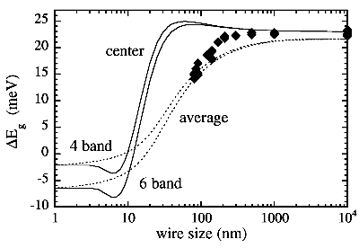
Fig. 11: Comparison of the calculated energy gap shift, averaged over the wire cross section, with the photoluminescence peak position for lateral wire width between 80 and 1000 nm. For comparison the gap in the center of the wire is shown for 6-band and 4-band calculation.
X-Ray Investigations
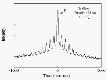
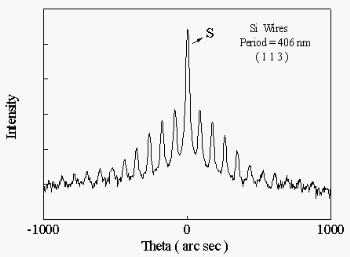
The structural parameters of the Si/SiGe multiquantum well layers were studied by employing x-ray diffraction techniques, like double and triple crystal diffractometry. In Figs. 12a and b (311) w-scans are shown for two Si-wire samples, with identical period (glancing angle exit diffraction). For the sample shown in Fig. 12a, the etching time was 13 min, for the sample shown in Fig. 12b it was 17 min. Since the number of wire satellites in Fig. 12b is somewhat larger, the structural quality of the periodic wire structures has certainly been improved.
|
|
|
Fig. 12: w -scans (113 reflection) of Si wire structures (area filling factor 0.5, period 406 nm) for RIE exposure times of 13 and 17 min, respectively)
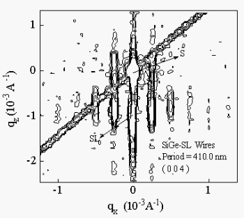
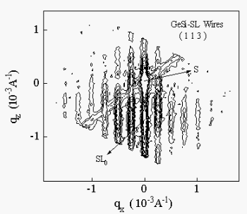
Reciprocal spacemaps around the (004) and the (311) reflection were recorded for the etched Si/SiGe multilayer samples (sample code: SiGe 46, which was grown by Stefan Zerlauth in the SiGeC MBE apparatus in Linz) as shown in Figs. 13a and 13b. Not only the MQW structure was etched through, but also part of the Si-buffer layer has been etched, as evidenced from the satellites accompanying the substrate peak marked by S. The MWQ structure gives rise to a superlattice peak (SLo) which is accompanied along the qx-direction by wire satellites. The period from the wire satellites is about 410 nm. A strain analysis based on these data will be performed.
|
|
|
Fig. 13: (004) and (113) reciprocal space maps of a Si/SiGe wire structure (period 410 nm).
Silicon Technology
(F. Schäffler, G. Steinbacher)
For an implementation of Si-based device structures it is important to remain compatible with standard Si technologies as far as possible. Because the chemistry of Si1-xGex and Si1-yCy layers is very similar to that of Si, many process sequences can be utilized without modification. However, processes employing high temperatures, such as post-implantation annealing or high temperature thermal oxidation, have to be adjusted toward low thermal budgets to account for the metastability of most Si-based heterolayer sequences. Thus heterodevices will have to utilize, and also may promote, a general trend toward lower processing temperatures, which is driven by leading-edge VLSI circuits, where the critical submicron feature sizes are jeopardized by thermal diffusion processes during high temperature steps.
For the development of Si-compatible, low-thermal-budget processing modules, as well as for a quick characterization of the electronic properties of epi-layer sequences, a versatile test layout with five mask layers was developed. The test elements reach from a simple transmission line arrangement for the assessment of the sheet and contact resistances of implanted and annealed ohmic contacts and variable-geometry Schottky diodes for an evaluation of Schottky barrier heights and periphery leakage currents, to gated multi-contact Hall bars and simple mesa-type FETs with variable gate lengths. The process sequence involves a self-aligned mesa etching step, which is essential for the gated Hall structures. All mask layers use a positive layout, which requires a image reversal photo resist (such as AZ5218) for the mesa process. Minimum feature sizes for optical contact lithography are 1µm, and additional marks for e-beam alignment are provided, which will allow the implementation of sub-micron gate lengths.
A complete processing sequence based on the five-layer layout was developed, which uses ion implantation and reactive ion etching for lateral structuring of the heterostructures, and — presently — lift-off processes for the metallization layer. Fig. 14 shows a cross-sectional view of an AZ5218 pattern with submicron feature size, which was achieved by controlled underexposure and appropriate development of the resist.
Fig. 14: Sub-micron resist pattern realized in image reversal resist AZ5218
X-Ray Diffractometry and Strain Analysis of Low-Dimensional Semiconductor Structures
(A.A. Darhuber, J. Stangl, S. Zerlauth, G. Bauer)
Strain relaxation in lattice mismatched systems has recently attracted a lot of attention with the increased application of strained layers in microelectronic and optoelectronic systems. There are in general two routes for strain relaxation: (i) plastic relaxation through misfit dislocation formation and (ii) elastic relaxation through a strain induced transition from a two dimensional planar growth mode to a three dimensional island morphology (as it is possible for compressively strained epilayers like Ge on Si or InAs on GaAs).
The strain induced islanding (Stranski-Krastanow growth mode) has found of lot of interest since it provides a possible mechanism for the formation of self-assembled quantum dots. Whereas changes of the surface morphology were already thoroughly studied and the conditions to control the size distribution and the self organizing behavior of the islands are rather well known, direct information on the strains and their relaxation is still lacking. These data are required for a proper interpretation of the electronic properties of such self-assembled dots. Therefore, we have been studying the structural properties of Ge dot multilayers embedded in Si (grown by MBE both at the Walter Schottky Institut as well as in Linz by S. Zerlauth) as well as of InAs dot multilayers in GaAs (grown at the Ioffe Institute St. Petersburg and at the Technical University Berlin) by x-ray diffraction techniques (reciprocal space mapping around symmetrical and asymmetrical reflections) and by x-ray reflectivity in Linz, at the ESRF Grenoble as well as at the Hasylab at DESY, Hamburg.
A typical cross sectional transmission electron microscopy micrograph of a SiGe dot multilayer is shown in Fig. 15, giving clear evidence for partial vertical ordering of the dots, as induced by strain fields. In addition to vertical ordering, lateral ordering in the (001) growth plane occurs as well, driven by the orientational dependence of the Young’s modulus in this plane. For both Ge and InAs, the polar diagram of Young’s moduli exhibit smaller values than that of the corresponding Si or GaAs matrix, with minima along the two orthogonal [100] and [010] directions.
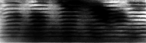
Fig. 15: Cross-sectional TEM, SiGe dot multilayer in Si (SiGe51).
So far from x-ray diffraction and reflectivity measurements the following information could be obtained:
(i) average values for the strain relaxation within the Ge dots in multilayers, as well as for the asymptotic strain in the Si matrix;
(ii) degree of vertical ordering of the dots in multilayers;
(iii) lateral ordering of the dots in the (001) plane in a square array along the [100] and [010] directions for Ge and InAs dots.
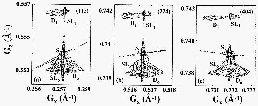
Fig. 16: Asymmetrical reciprocal space maps around the (113) (a), (224) (b), and (404) (c) reciprocal lattice points.
Figure 16 shows as an example the diffusely scattered intensity around (113), (224) and (404) reciprocal lattice points from a 19 period Ge dot multilayer sample (d = 30 nm). The diffusely scattered intensity comes from strained Si matrix regions (mainly around the central superlattice SL0 peak) as well as from the dot region itself (SL1).
More detailed investigations of the strain fields require:
(i) model calculations based on the finite element method or on the valence force model
(ii) grazing incidence diffraction measurements.
Acknowledgments
The investigations were further supported by several funding organizations like Fonds zur Förderung der wissenschaftlichen Forschung, Vienna, the Österreichische Nationalbank, the Projektforschung des BMWVK, and the Daimler Benz Research Organisation.
References
[1] for an overview see e.g. E. Kasper and F. Schäffler, Semiconductors and Semimetals Vol. 33, chapter 4, Academic Press, Boston 1991
[2] for an overview see e.g. A. Gruhle, Springer Series in Electronics and Photonics Vol. 52, chapter 4, Springer, Berlin 1994
[3] for an overview see e.g. U. König and F. Schäffler, Proc. Int. Conf. Solid State Devices and Materials (SSDM), Jap. Soc. Appl. Physics, Chiba 19993, p.201
[4] for an overview see e.g. H. Presting, H. Kibbel, M. Jaros, R.M. Turton, U. Menczigar, G. Abstreiter, and H.G. Grimmeiss, Semicond. Sci. Technol. 7, 1127 (1992)
[5] E.A.Fitzgerald, Y.-H. Xie, M.L. Green, D. Brasen, A.R. Kortan, J. Michel, Y.-J. Mii, and B.E. Weir, Appl. Phys. Lett. 59, 811 (1991)
[6] F.K. LeGoues, B.S. Meyerson, and J.F. Morar, Appl. Phys. Lett. 66, 2903 (1991)
[7] F. Schäffler, D. Többen, H.-J. Herzog, G. Abstreiter, and B. Holländer, Semiconductor Sci. Technol. 7, 260 (1992)
[8] K. Eberl, S.S. Iyer, and F.K. LeGoues, Appl. Phys. Lett. 64, 739 (1994)
[9] K. Brunner, K. Eberl, and W. Winter, Phys. Rev. Lett. 76, 303 (1996)
[10] K. Brunner, W. Winter, and K. Eberl, Appl. Phys. Lett. 69, 1279 (1996)
[11] F. Schäffler, M. Wachter, H.-J. Herzog, K. Thonke, and R. Sauer, J. Cryst. Growth 127, 411 (1993)
[12] L.P. Tilly, P.M. Mooney, J.O. Chu, F.K. LeGoues, Appl. Phys. Lett. 67, 2488 (1995)
[13] M.A. Haase, J. Qiu, J.M. DePuydt, H. Cheng, Appl. Phys. Lett. 59, 1272 (1991).
[14] H. Jeon, J. Ding, W.R. Patterson, A.V. Nurmikko, W. Xie, D.C. Grillo, M. Kobayashi, R.L. Gunshor, Appl. Phys. Lett. 59, 3619 (1991).
[15] D.A. Faux and J. Haigh , J. Phys.: Condens. Matter 2, 10289 (1990).
[16] M. Grundmann, O. Stier and D. Bimberg, Phys. Rev. B 50, 14187 (1994).
[17] L. De Caro and L. Tapfer, Phys. Rev. B 51, 4374 (1995).
[18] C.G. Van de Walle, Phys. Rev. B 39 1871 (1989).
[19] E.O. Kane in Semiconductors and Semimetals, Ed. R.K. Willardson and A.C. Beer, Vol. 1, Academic Press, New York 1966.
[20] L. De Caro and L. Tapfer, Phys. Rev. B 51, 4381 (1995).
[21] G.L. Bir and G.E. Pikus, in "Symmetry and strain induced effects in semiconductors", John Wiley, New York 1974.
[22] J. Singh, in Handbook on Semiconductors, Ed. T.S. Moss, Vol. 2 by M. Balkanski, (Elsevier Science, Amsterdam 1994), p. 235ff; J. Singh, in Physics of Semiconductors and their Heterostructures, Ed. Anne T. Brown, (McGraw-Hill, Amsterdam 1993), p. 218ff.
[ 23] A.A. Darhuber, V. Holy, J. Stangl,G. Bauer, P. Schittenhelm, G. Abstreiter: "Structural investigations for self assembled Ge dots by x-ray diffraction and reflection", Thin Solid Films, in print.
[ 24] A.A. Darhuber, V. Holy, J. Stangl,G. Bauer, P. Schittenhelm, G. Abstreiter: "Interface roughness in strained Si/SiGe multilayers", Materials Research Society, Boston , 1996, in print.
[ 25] A.A. Darhuber, V. Holy, J. Stangl, G. Bauer, A. Krost, F. Heinrichsdorff, M. Grundmann, D. Bimberg, V.M. Ustinov, P.S. Kopev, AS.O. Kosogov, P. Werner: "Lateral and vertical ordering in multilayered self-organized InGaAs quantum dots studied by high resolution x-ray diffraction", Appl.Phys.Lett., in print.
Project Information
Project Manager
Univ.-Prof. Dr. Günther Bauer
Institut für Halbleiterphysik, Johannes Kepler Universität Linz, A-4040 Linz
Project Group
|
Last Name |
First Name |
Status |
Remarks |
|
Brunthaler |
Gerhard |
Ph.D. |
|
|
Darhuber |
Anton |
dissertation |
|
|
Fünfstück |
Britta |
diploma student |
|
|
Grill |
Thomas |
diploma student |
|
|
Helm |
Manfred |
assistant professor |
|
|
Kruck |
Peter |
dissertation |
|
|
Li |
Jianhua |
Ph.D. |
|
|
Penn |
Christian |
dissertation |
|
|
Prinz |
Adrian |
dissertation |
|
|
Schäffler |
Friedrich |
associate professor |
|
|
Seyringer |
Heinz |
dissertation |
|
|
Stangl |
Julian |
dissertation |
|
|
Steinbacher |
Günther |
diploma student |
|
|
Straub |
Hubert |
dissertation |
GMe funding |
|
Zerlauth |
Stefan |
dissertation |
|
|
Zhuang |
Yan |
dissertation |
Books and Contributions to Books
Publications in Reviewed Journals
Presentations
Doctor’s Theses
Cooperations