Backside-Laserprober Technique for Characterization of Semiconductor Power Devices
N. Seliger, C. Fürböck, P. Habaš, D. Pogany, E. Gornik
Institute of Solid State Electronics &
Center of Microstructure Research (MISZ),
TU Wien, A-1040 Vienna, Austria
An infrared laserprobe technique for the characterization of the self-heating in the µs range in power VDMOSFETs and IGBTs is presented. Based on the thermo-optical effect in silicon, this technique detects interferometrically the temperature induced changes of the silicon refractive index. The time evolution of the lattice temperature in the device active region is studied for the power devices biased under shorted load conditions. Optical experiments are combined with electro-thermal device modeling and electrical characterization. From the calculated phase modulation signals fitted to the experiments a value for temperature coefficient of the refractive index of 1.6·10-4 K-1 is found which is in good agreement with the literature.
The steady increase of the switching frequency of power semiconductor devices under high voltage and current conditions causes transient thermal effects to become a more severe and critical issue. Although much attention has been given to thermal effects in power devices, there are so far no experimental techniques available for a time-resolved analysis of destructive thermal effects in dynamic device operation. In this paper we present the application of the backside laserprobe technique [1] to analyze the transient heating in power Vertical Double-diffused (VD)MOSFETs and in Insulated Gate Bipolar Transistors (IGBTs) biased under shorted load conditions.
Optical Technique
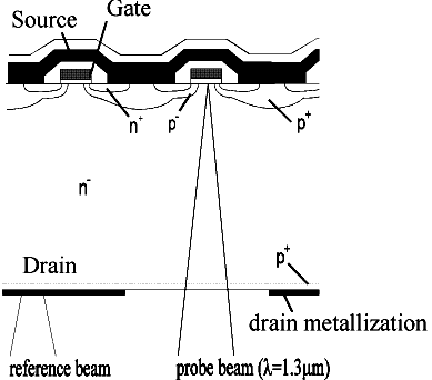
The principle of the laserprober set-up is demonstrated in Fig. 1. An increase in the refractive index of silicon due to the lattice heating (thermo-optical effect) in dynamic device operation modulates the phase of the laser probing beam. The probing beam reflected from the gate and a reference beam reflected from the drain metallization interfere in a photodetector. The electrical signal at the detector corresponding to the thermally induced phase change is recorded and averaged by a digital oscilloscope. Since the photon energy of the laser beam (l = 1.3µm) is below the energy gap of silicon, the optical measurements have no impact on the device electrical characteristics.
The laserprobe measurements were performed on commercially available VDMOSFETs of 150 V and 200 V breakdown voltage, and on IGBTs with 1200 V breakdown voltage. In VDMOSFETs, optical access through the drain contact is obtained after mechanical removal of the original contact metallization, polishing the substrate and evaporation of a thin Ti-Au film leaving a small square window opened. This preparation does not change the device performance, but induces a small drain contact resistance. For measurements on IGBTs, the device preparation is different as mechanical contact removal would also destroy the p+-anode layer of the IGBT. We have therefore developed a process technique which allows selective etching of the small window (100 µm x 100 µm) into the contact metallization. The etching stops just at the silicon surface (Fig. 1) which ensures the proper functionality of the device.
Fig. 1: Laserprobe method for the detection of the transient lattice heating in power devices. The probing laser beam (beam diameter of 8 µm) is focused through a small window in the drain contact on a single IGBT (or VDMOSFET) cell and is reflected from the polysilicon gate. The interferometer reference beam is placed at the metallization.
Experiments
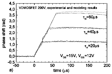
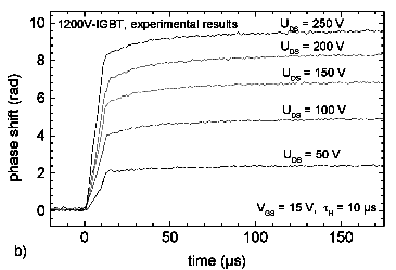
In the experiments on VDMOSFETs, the amount of the transient lattice heating is controlled by applying pulses with different pulse levels from VGS = 0 V to 8 V and 12 V and different pulse widths tH (5 µs to 60 µs) to the gate. The drain-to-source bias is held constant at VDS = 15V. The transient drain current is monitored by a voltage drop across a resistor connected in series with the drain. The power dissipation in IGBTs is controlled by the drain-to-source voltage ranging from 50 V to 400 V. The device is switched by gate pulses of 15 V height and length of 10 µs. Here the transient current is measured inductively by means of a current probe. In both cases the pulse repetition frequency is chosen to 10 Hz, in order to enable total device cooling between subsequent pulses. Figure 2 shows typical results for the transient phase signal obtained from laserprobe experiments on VDMOSFET and IGBT. During the heating the phase signal increase is linear in time. After heating turn-off, the phase signal remains almost constant in the first 100 µs. In that case, the peak temperature decreases and simultaneously, the heat propagates into the silicon well. Therefore, the length where the temperature changes (the beam modulation length) increases. As the phase change is proportional to the integral of the temperature increase along the beam modulation length, the resulting phase signal is nearly constant.
Besides the thermo-optical effect, the phase of the laser beam is also modulated due to the free-carrier effect [2]. We have found that this effect can be neglected both in VDMOSFETs and IGBTs. Performing optical measurements on VDMOSFETs with VDS = 0 V and applying pulses to the gate (no device heating), the resulting phase signal is close to the detection limit of the measurement set-up. A similar experiment has been carried out on IGBT with a drain-to-source voltage of VDS = 2 V. Even under this low power condition the thermally induced phase signal dominates and superimposes the free-carrier signal.
|
|
|
Fig. 2: Laser-probe measurement results for the time-resolved phase shift on a) 200V-VDMOSFET and b) 1200V-IGBT. Pulse widths tH are indicated. The phase shift calculated for a value of the temperature coefficient of the refractive index of dn/dT = 1.6·10-4 K-1 of silicon is shown for VDMOSFET device (dotted line).
Numerical Modeling
The study of time dependence of the temperature in power devices requires modeling of the total chip consisting of several hundred cells including the chip package. To reduce the complexity of the model, we first analyzed the temperature distribution in a single VDMOSFET cell. The electrical characteristics of a single cell are calculated by a modified version of MINIMOS 6 [3]. The transient temperature profile is then obtained by numerically solving the 2-D heat conduction equation. The temperature distribution along the wafer depth (Fig. 3) at the center of the chip area is taken as input for modeling of the laser beam modulation.
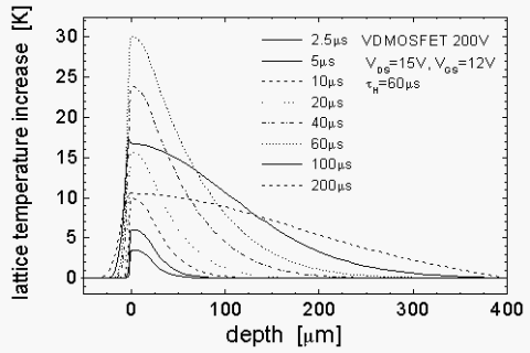
Fig. 3: Numerical modeling result of the transient temperature profile across the chip center (200V VDMOSFET).
The transient phase modulation signals are calculated by the application of the transmission-line model presented in [4], which has been extended including the lattice heating. The phase change obtained from the rigorous transmission line model is very close to that calculated from the temperature profile using a simple geometric optic approach. This implies that the geometric optic approach can be accurately used, which significantly reduces the complexity in the optical data interpretation. A direct comparison of the numerical modeling results and the phase shift from measurements is possible only if the exact value of the temperature coefficient of the refractive index of silicon (dn/dT) is known. On the other hand, assuming that accurate modeling results are provided, the dn/dT can be determined by the calibration of the experiments. For the purpose of the verification of numerical analysis, the channel temperature at various heating pulse widths tH is extracted from pulsed I-V measurements (Fig. 4).
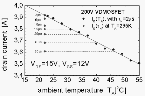
Fig. 4: Pulsed I-V measurements for the determination of the channel temperature for different heating pulse widths (200 V VDMOSFET). The channel heating at short pulses tH = 2 µs (circles) at increased ambient temperature is used as a reference. From the decreased drain current due to self-heating with longer gate pulses (diamonds) the corresponding channel temperature is extracted.
The modeling results for the temperature close to the Si/SiO2-interface correspond to the values obtained from the pulsed I-V measurements. As depicted in Fig. 4 for a heating pulse width of tH = 60 µs, the temperature increase in the channel after 20 µs is extracted to DT = 12.5 K, in agreement with the calculated value of DT = 12 K. Quantitative matching of various modeling to measurement results of the transient phase shift at the end of the heating period results in a mean value across all samples of dn/dT = 1.6·10-4 K-1, where this result is very consistent with data from the literature [5]. Figure 2a shows a typical result for the calculated phase signal which is in good agreement with the experiment.
Conclusion
The backside laserprobe technique has been successfully applied to study the transient heating in power VDMOSFETs and IGBTs with a high temporal resolution. From the numerical analysis a 1-D thermal model combined with a geometric optic approach are found to be sufficient for the modeling of the phase modulation signals. From this study a value of dn/dT is obtained, which is the basis for quantitative studies of the critical thermal effects in such devices.
Acknowledgments
This work was partly supported by the "Bundesministerium für Wissenschaft und Forschung". The authors would like to thank Dr. G. Deboy (SIEMENS Munich) for providing IGBT samples and fruitful discussions.
References
[1] M. Goldstein, G. Sölkner and E. Gornik: "Heterodyne interferometer for the detection of electric and thermal signals in integrated circuits through the substrate", Microelectr. Eng., Vol. 24, pp. 431 – 436, 1994.
[2] R. Soref and B. Benett: "Electrooptical effects in silicon", IEEE J. Quantum Electr., Vol. QE-23, No. 1, pp.123 – 129, Jan. 1987.
[3] Group of authors: "MINIMOS 6 - User’s guide", Institute for Microelectronics,
TU Vienna, Austria, 1995.
[4] N. Seliger, P. Habaš and E. Gornik: "Modeling and measurements of backside laser-probe signals in MOSFETs", in Proc. ESSDERC’95, The Hague (NL), Sept. 1995, pp. 773 – 776.
[5] M. Bertolotti, V. Bogdanov, A. Ferrari, A. Jascow, N. Nazorova, A. Pikthin, L. Schirone, "Temperature dependence of the refractive index in semiconductors", J. Opt. Soc. Am. B., Vol. 7, No. 6, pp. 918 – 922, June 1990.
Project Information
Project Manager
Univ.-Prof. Dr. Erich Gornik
Institut für Festkörperelektronik, Technische Universität Wien, A-1040 Vienna
Project Group
|
Last Name |
First Name |
Status |
Remarks |
|
Fürböck |
Christoph |
dissertation |
|
|
Gornik |
Erich |
university professor |
|
|
Habaš |
Predrag |
postdoc |
|
|
Pogany |
Dionyz |
guest scientist |
|
|
Seliger |
Norbert |
dissertation |
Publications in Reviewed Journals
Presentations
Doctor’s Theses
Cooperations