High Precision Depth Profiles with SIMS
H. Hutter and K. Piplits
Institute of Analytical Chemistry, TU Wien
A-1060 Vienna, Austria
This paper demonstrates applications of surface analysis techniques for the investigation and characterization of materials and production processes. SIMS depth profile measurements of implanted erbium in silicon demonstrate that high precision measurements of low concentrations are necessary to assist implantation and simulation groups. Measurements of potassium profiles in fullerene films were performed to investigate diffusion processes in order to optimize material properties. Measurements of the three dimensional distribution of trace elements in high purity molybdenum points out the importance of distribution analysis of raw materials for microelectronics.
Introduction
Surface analysis techniques play an important role for supporting material development and process optimisation. One of the most common techniques is Secondary Ion Mass Spectrometry (SIMS). This is due to the high detection power of the method, the fact that all elements are detectable and the possibility of registering two- and three dimensional distributions of trace elements.
To support various investigations in the field of microelectronics, the performance of analytical methods has to be increased. The actual questions of technology demand a permanent development of the precision of measurements, especially at very low concentrations. The supervision of the implantation process stability by measurements of depth profiles for erbium demonstrates the support of optimizing production processes. Investigation of the implanted potassium distribution in C60 fullerenes supplies information for the development of new materials. It will be shown that the determination of trace element concentration is necessary for the development of high purity materials like molybdenum.
Erbium in Silicon
The 4f shell of rare earth elements is well shielded by the outer shell electrons. Therefore these elements exhibit sharp and almost atom-like spectra when incorporated as dopants in semiconductors and isolators. The emitted wavelengths practically coincide with those observed for isolated atoms and depend only little on the host material. Erbium implanted into Si produces rich spectra of sharp lines in photo- and also in electroluminescence in a narrow spectral region close to 1,54 µm. This wavelength stimulates interest in Si:Er as a candidate for light emitting devices for fibreoptic communication systems and also for on-chip and inter-chip optical data transfer.
Investigations by high resolution photoluminescence and deep level transient spectroscopy of Er-implanted silicon were made by Dr. Palmetshofer [1].
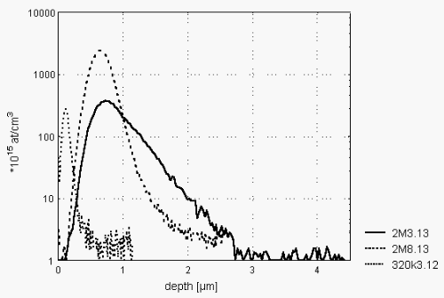
The ion implantation of 320 keV (implanted by Dr. Palmetshofer, University Linz) and 2 MV (implanted in Guildford, UK) erbium in CZ and FZ silicon was performed at room temperature with doses of 3,13·1013 and 8,13·1013 cm-2. To determine the diffusion coefficient of erbium in silicon, one series of the samples were tempered at 900 °C for 30 min in nitrogen.
The SIMS depth profiles of implanted erbium in silicon show no broadening of the erbium implantation profiles during the temperature treatment. The maximum concentration of erbium was about 2·1018 atoms per cm3, the profiles were Gaussian like. The detection limit was lower than 1·1015 atoms per cm3. This indicates that there is no significant diffusion of erbium at a temperature of 900 °C.
The profiles show no enrichment of Er at the surface, this indicates that Er does not segregate during the annealing in samples with implantation doses below 1014 cm-2.
Fig. 1: SIMS erbium profiles of Si implanted with 2 MeV (2M3.13, 2M8.13) and 320 keV (320k3.12) Er+ with doses of 3.13·1013 cm-2 (2M3.13), 8.13·1013 cm-2 (2M8.13) and 0.312·1013 cm-2 (320k3.12). All profiles show the expected gaussian distribution.
Contrary to all expectations the profiles of the first measured 2 MeV samples were channeling like. Further analysis shows that these profiles are not results of axial channeling in [100] direction but of planar channeling. Probably this is the result of an incorrect implantation process. Renewed implantations did not show this behavior.
K in Fullerens
Films of chromatographically purified C60 were prepared on silicon substrates by vacuum deposition. Ion implantation of 30 keV 39K+ was performed at 300 °C in a vacuum better than 10-4 Pa. The depth profiles were measured using 5.5 keV O2+ primary ions.
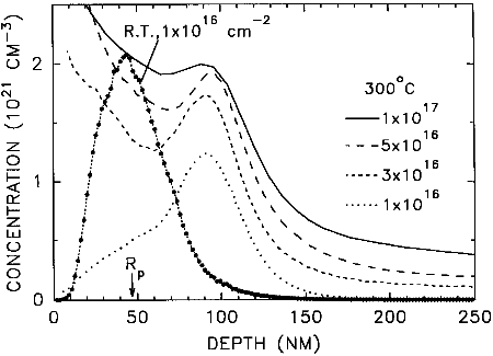
Fig. 2: SIMS potassium profiles for C60 films implanted with 30 keV K+ at room temperature (1·1016) and at 300 °C (1, 3, 5 and 10·1016 cm-2).
Figure 2 shows the depth profile of 39K+ for samples implanted with 30 keV at room temperature (1·1016 cm-2) and at 300 °C (1, 3, 5 and 10·1016 cm-2). For room temperature implantation, the experimental profile is Gaussian-like with a weak diffusion induced tail at greater depths.
At 300 °C implantation temperature a peak appears in the tail region at about 100 nm, and the K-concentration within the theoretical ion range is strongly reduced. An increase of the dose leads to a subsequent increase of the peak at about 100 nm and to a slight shift of its maximum into the depth. However, with increasing dose the K-concentration in this region tends to saturate at a value of about 2·1021 cm-3. A certain amount of K diffuses out to the surface, but the diffusion into the depth is more pronounced. In all samples more than 70% of the implanted atoms are found underneath a 70 nm surface layer. Raman spectra indicate that there is a passivating a-C surface layer and the accumulation of K is at the a-C/C60 interface. These structures may have useful applications for new Tc superconducting devices on the basis of fullerenes which can be handled on air [2].
Ultra pure Molybdenum
Due to the high heat resistivity molybdenum is used as sample holder for the MBE process. During the MBE process trace elements with concentration below the ppm (part per million) level diffuse in the sample, this results in contamination of the devices. The use of ultra pure materials prevents this process. Not only the overall (bulk) concentration is decisive for this diffusion, also the distribution and the chemical state of the trace elements. Therefore the determination of the three dimensional distribution is necessary for the development of functional materials.
The material we investigated is 6N molybdenum, that means that the concentration of all trace elements together is below 1 ppm (part per million). This material is used for the production of MBE sample holders.
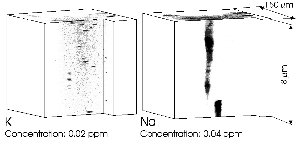
Fig. 3: 3D-distributions of K (left side) and Na (right side) in high purity molybdenum (6n purity). The K precipitates have diameters about 30 nm, the Na is concentrated in impurities with a diameter of about 1 µm.
The investigations indicates that the trace elements are concentrated in precipitates with diameters depending on the measured element. There is no correlation between the different species, this indicates that these elements are not present due to contamination during the production process.
Conclusion
Microelectronics is a continual challenge for modern material analysis. In many cases improvements of well established analytical methods, like SIMS, is necessary to obtain precise measurement results of the concentration of dopands and trace elements. This knowledge makes the development of new processes and materials possible.
[1] W. Jantsch, L. Palmetshofer: "Erbium Related Centres in Silicon", Grundlagen und Technologic elektronischer Bauelemente, Großarl 1995, ISBN 3-901578-01-3
[2] J. Kastner, H. Kuzmany, L. Palmetshofer, K. Piplits: "Formation of air stable buried K-fulleride layers by ion implantation", Synthetic Metals 70 (1995) 1469 – 1470
[3] L. Palmetshofer, M. Geretschläger, J. Kastner, H. Kutzmany, K. Piplits: "Characterization of K-fulleride layers formed by ion implantation", J. Appl. Phys. 77 (3), 1995
[4] H. Hutter, Ch. Brunner, St. Nikolov, Ch. Mittermayr, M. Grasserbauer: "Imaging surface spectrometry for two and three dimensional characterization of materials", Fresenius J Anal Chem (1996) 355:585 – 590
Project Information
Project Manager
Univ.-Ass. Dr. Herbert Hutter
Institute of Analytical Chemistry, Vienna University of Technology, A-1040 Vienna,
Project Group
|
Last Name |
First Name |
Status |
Remarks |
|
Brunner |
Christian |
dissertation |
|
|
Fischer |
Harald |
diplom thesis |
|
|
Hutter |
Herbert |
Assistance Professor |
|
|
Piplits |
Kurt |
technician |
partial GMe funding |
|
Wolkenstein |
Martin |
dissertation |
Publications in Reviewed Journals
Presentations
Cooperations