Characterization of Si-based Structures by Luminescence and ESR Experiments
W. Jantsch, S. Lanzerstorfer, M. Stepikhova, L. Palmetshofer
Institut für Halbleiterphysik, Johannes Kepler Universität,
A-4040 Linz, Austria
Bulk Si, quantum-well structures of SiGe, and porous Si structures have been investigated by luminescence and electron-spin-resonance (ESR) methods. In luminescence we find after implantation and thermal treatment residual impurities with finger-print spectra and also dislocation related structures. The latter are distinguishable from other defects by their characteristic dependence on hydrostatic pressure and temperature. In ESR experiments, cyclotron resonance is clearly visible, which offers the possibility to detect free carriers without the need for contacts.
Introduction
Among the current problems in the technology of Si there is (i) the development and the integration of light emitting elements [1], [2] and (ii) the development of ultra-small ultra-fast devices. In both cases, small structures are used and effective characterization methods are needed to identify residual defects, carrier concentration and their mobility, dimensionality of the structure, etc. In many cases, electrical contacts impose substantial problems in such structures and therefore contactless methods are preferred if available. Among the standard methods for the characterization of defects is photo-luminescence which in high quality crystals can detect defect concentrations as low as 1010 cm-3, in some cases sufficient also for low-dimensional samples. The spectra reveal their origin, however, only in rather specific cases. Electron spin resonance (ESR) in principle is more powerful since it yields information also on the chemical identity of the defect and its neighbors. On the other hand, ESR relies on the absorption of microwaves which penetrate the whole sample and thus its sensitivity is rather described by an absolute number of spins which for typical defects in Si is of the order of 1012, too large for small structures. The sensitivity for free carriers in ESR can be much bigger, a few thousand electrons can be easily detected in cyclotron resonance if the mobility is high enough as it was demonstrated in the course of this project.
In this paper we concentrate on two examples of luminescence results. Some of the luminescence spectra seen exhibit sharp, characteristic patterns due to phonon replica and their isotope splittings, constituting a fingerprint of the defect species. Copper, e.g., is clearly seen and detectable as a frequent contamination after even simple technological steps. Other luminescence spectra produce rather wide and less characteristic features and sometimes they are not clearly distinguishable from other luminescence centers. As an example, we present data obtained on Er-implanted samples which show, after specific treatment, meant for annealing of implantation defects, a strong emission [4] close to the technically interesting wavelength of 1.54 µm. We show that this emission at low temperature really is due to Er, but at temperatures above 150 K, luminescence due to dislocations prevails.
In part 3 we present photoluminescence data on porous Si which was doped electrolytically by Er. We observe emission of the characteristic 1.54 µm emission of Er even above room temperature although in bulk Si it is quenched already below 200 K.
Photoluminescence Due to Dislocations on Doped Si
Although Si plays the dominant role in microelectronics, it suffers for principle reasons in optoelectronic applications: Because of its indirect gap it does not permit the fabrications of band edge emitters in contrast to III-V and II-VI compounds. In the past few years, possibilities to overcome this shortcoming were investigated making use of luminescence due to localized states. One idea in this context was to utilize the intra-4f transitions of rare earth elements, and here in particular those of Er, whose lowest transition occurs at 1.54 µm, close to the damping minimum of silica fibers [4]. In the past few years, the weak luminescence yield was optimized but a principle problem still appears unsolved: the luminescence quenches at temperatures well below room temperatures, excluding technical application [3]. More recently, however, reports appeared, claiming electroluminescence also at room temperatures due to Er in Si. In order to clarify the origin of this luminescence we have investigated samples which show luminescence close to 1.5 µm also at 300 K.
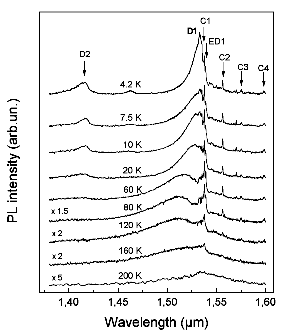
Fig. 1: Photoluminescence spectra of Er-implanted CZ-Si as a function of different temperatures.
The nature of this emission is more clearly seen in low temperature experiments. In Fig. 1, luminescence spectra are shown obtained in CZ-Si implanted with Er (2 MeV, 3× 1013 cm-2) after annealing at 900 °C for 30 min. At low temperatures, the emission due to interstitial (cubic) Er is seen (lines marked C1…C4) together with a line due to an Er complex [5]. In addition, a wide structure is seen close to 1.5 µm which, together with the line marked D2 is attributed to dislocations in the literature. The structure at 1.5 µm, known as D1 line in the literature [6], exhibits also a characteristic temperature shift — at low temperatures towards shorter, above 80 K towards longer wavelengths — whereas the Er line positions remain independent of temperature owing to the extremely localized nature of the 4f states.
Another characteristic feature of the Er lines is their independence on pressure which allows to distinguish them easily from the dislocation luminescence. This is shown in Fig. 2, where low temperature spectra are given for different hydrostatic pressure. It is clearly seen that the D-lines shift towards shorter wavelength whereas the Er lines remain independent of pressure. The pressure coefficient for the transition energy is evaluated to be -2.3 meV/kbar which may serve as an additional characteristic feature of the dislocation luminescence.
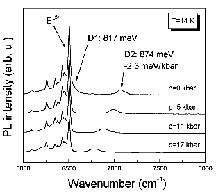
Fig. 2: Luminescence spectra of CZ Si:Er for pressures of 0, 5, 11, and 17 kbar, respectively. The highest pressure corresponds to the lowest D2 position.
The dislocation luminescence is seen also in electroluminescence devices designed for Er emission. Junctions prepared by implanting Er into p-type Si exhibit the same type of electroluminescence spectra when operated under forward bias condition as shown in Fig. 1, i.e., they give strong Er luminescence at low temperature but above 150 – 180 K only the dislocation emission is seen.
Luminescence of Porous Si:Er
The temperature induced quenching of the Er luminescence in different host materials seems to correlate to the energy gap of the host: the bigger the energy gap, the higher the critical temperature for quenching. Therefore, in order to improve the luminescence yield, any measure to increase the gap of Si based material should help. In order to test this hypothesis, we have produced porous Si by anodic etching. Porous Si consists of single crystal material with pores and columns of about 40 Å in diameter. Porous Si has been investigated in the last few years because of its bright visible photo- and electroluminescence which is interpreted in terms of the blue shift of the band edge emission due to electronic confinement in the small structures.
We introduced Er into po-Si electrolytically from ErCl3 dissolved in ethanol. After annealing at 1000 °C for 10 s in an O2/N2 atmosphere the samples show sharp and intense Er-related emission which can be clearly demonstrated by excitation spectroscopy: The emission of the 1.54 µm can be excited resonantly both in the 870 and the 980 nm bands, which correspond to the transitions from the J=15/2 ground state of Er to the 9/2 and the 11/2 states, respectively. In bulk Si, these excitations are not detectable because of the strong competition of the interband transitions — these transitions are situated already above the gap of single crystal Si.
In Fig. 3 we show the temperature dependence of our po-Si:Er emission at 1.54 µm as a function of temperature in comparison to other Si-based host material. The dramatic improvement as compared to single crystal bulk Si is clearly seen which again demonstrates the empirical rule of Favennec [3].
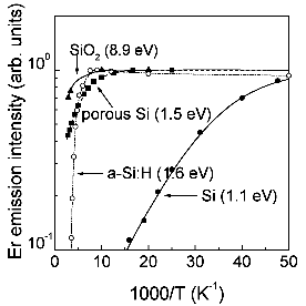
Fig. 3: Normalized luminescence yield of Er in Si-based material as a function of inverse temperature for bulk Si, amorphous Si, po-Si and SiO2.
Conclusions
In this report we have shown that the technologically interesting luminescence of Er in Si can be improved dramatically at high temperatures by using Si-related material with larger energy gap: In agreement with the rule of Favennec, the thermal quenching of the Er luminescence occurs at higher temperatures for material with higher energy gap. Porous Si provides one of very few possibilities so far to increase the gap of Si (the alloys of Si have a tendency for smaller gaps only). Reports in the literature on room temperature Er emission in electro-luminescence of forward biased p-n junctions should be reconsidered in view of our present results which show that the emission observed in our samples are due to dislocations at elevated temperature.
References
[1] W. Jantsch, H. Przybylinska, C. Skiebiszewski, S. Lanzerstorfer, L. Palmetshofer (invited): "Factors, governing the photoluminescence yield of Erbium implanted Silicon", MRS proceedings 422, 101 (1996)
[2] W. Jantsch, H. Przybylinska (invited): "Rare Earth Luminescence in Semiconductors", Proc. XXIII. Int. Conf. Phys. Semiconductors, Berlin July 21-26, 1996, in press
[3] P.N. Favennec, H. l´Haridon, D. Moutonnet, M. Salvi, and M. Gauneau, Mat. Res. Soc. Symp. Proc. 301, 181 (1993)
[4] H. Ennen, G. Pomrenke, A. Axmann, K. Eisele, W. Haydl, and J. Schneider, Appl. Phys. Lett. 46, 381 (1985)
[5] H. Przybylinska, W. Jantsch, Yu. Suprun-Belevich, M. Stepikhova, L. Palmetshofer, G. Hendorfer, A. Kozanecki, R. J. Wilson, B. J. Sealy, "Optically active Erbium centers in Silicon", Phys. Rev. B54, 2532 (1996)
[6] R. Sauer, J. Weber, J. Stolz, E.R. Weber, K.-H. Küsters and H. Alexander, Appl. Phys. A36, 1 (1985)
Project Information
Project Manager
Prof. Wolfgang Jantsch
Institut für Halbleiterphysik, Johannes-Kepler-Universität, A-4040 Linz
Project Group
|
Last Name |
First Name |
Status |
Remarks |
|
Jantsch |
Wolfgang |
university professor |
|
|
Lanzerstorfer |
Sven |
dissertation |
15% GMe funding |
|
Palmetshofer |
Leopold |
associate professor |
|
|
Wirtl |
Elisabeth |
technician |
50% GMe funding |
Publications in Reviewed Journals
Presentations
Cooperations