UNICHIP Vienna, a Technology Transfer Center for ASIC Design
N. Kerö, G.R. Cadek, W. Kausel, E. Kowarsch, P.C. Thorwartl
Institut für Allgemeine Elektrotechnik und Elektronik,
TU Wien, A-1040 Vienna, Austria
T. Sauter
Institut für Computertechnik,
TU Wien, A-1040 Vienna, Austria
After a short description of the SME oriented work of UNICHIP a design of an analogue ASIC is presented. This project has been undertaken in close cooperation with and Austrian SME (Frequentis-Nachrichtentechnik) It serves perfectly well as an successful example of technology transfer of ASIC design and know-how.
Introduction
From its very beginning the work of the UNICHIP Wien design team was targeted towards technology transfer of ASIC design knowledge mainly to Austrian SMEs. Various measures were taken to achieve this goal. Firstly the undergraduate education of VLSI design methodologies has been intensified. Recently interesting diploma-theses have been completed such as a "Re-targetable VHDL-module for an SCSI-Controller" or "CULT – A new class of scaleable benchmark circuits for FPGAs".
For training and education focused directly towards SMEs we use various different approaches. Apart from front-end design courses which are held together with the University Extension Center, in-house training and consulting activities lasting between one and three days each have proved to be very successful. In the last two years more than 15 firms accepted this offer. Finally, projects performed in close cooperation with a partner from industry are by far the most effective way of technology transfer. In the remaining part of this report we shall describe such a transfer project.
Analog Headset Transceiver: A Technology Transfer Project
Together with Frequentis, an Austrian SME dealing with speech communication systems for air traffic control, an analogue headset transceiver ASIC was developed. Instead of focusing on design based training of Frequentis engineers, the authors tried to transfer knowledge on how to manage analogue IC design projects and to specify circuits to be developed and fabricated by sub-contractors. The cooperation started with a short product analysis study lasting no more than four weeks. As a result of this preliminary work, four areas suitable for replacing standard solutions with ASICs were spotted, one analogue and three digital designs of varying complexity. It was agreed to realize the analogue ASIC, this one being the most urgent.
The headset transceiver (HST) is basically the interface between the communication system and the air traffic controllers. Since each working place in a typical system has three sockets to which headsets can be connected, the first benefit expected from an integrated solution is a significant reduction of space on the printed circuit boards needed for the interfaces. Another advantage is the increased reliability. The third and somehow unusual benefit is a standardization aspect. Speech communication systems are unique solutions, and so far, despite a modular design of the digital parts of the system, the interface boards have been developed anew for each customer. An ASIC, however, is a fixed starting point for future designs and may thus help reduce also development costs.
Function of the HST
The basic function of the ASIC is the amplification and conditioning of the voice-band signals that come in from the headset’s microphone or are applied to the earphones, respectively. In addition, the presence of a headset must be detected. If no headset, or more precisely, no microphone, is attached to the module, then a loop-back function is to be activated such that the speaker hears his own voice, signaling him that his partner does no longer exist. This function is also useful for testing purposes because the complete signal path through the system — including the CODECs and most of the analogue amplifiers — may be monitored.
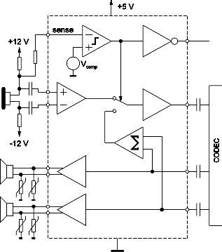
Figure 1 shows a block diagram of one channel of the HST together with the specifications. The ASIC actually comprises two of them. Since there is only a single supply voltage available, the drivers for the loudspeakers need differential outputs to meet the specifications. To be independent of the dc levels of the signals generated by the CODEC, capacitive coupling is used. Thus the internal reference potential could be set to its optimum value, which is derived from the supply with a simple resistive divider. An optional external capacitor connected to the divider improves the PSRR, and this analogue ground is carefully buffered to minimize crosstalk between the signals.
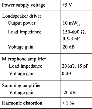
Fig. 1: Block diagram of HST together with electrical specifications.
Like all circuits in air traffic control applications, the whole system must comply with IEC 801-2-91, which requires the circuitry to withstand ESD pulses of 8 kV applied to its ports. Therefore all connections to the headset are protected by additional transient voltage absorbers. Unfortunately, these devices impose a significant capacitive load on the output drivers of the HST. Another important requirement is that for reliability reasons the drivers must survive shorts between the output terminals as well as between the outputs and ground (a typical cause of such a short is a mechanical damage of the headset cable).
The Course of the Project
As a first step a three months’ study was launched with the objective to evaluate the feasibility of this design from technical and economical points of view. As a result the following items could be delivered: an area estimation, design effort, possible ASIC manufacturers. It could be foreseen that the headset transceiver ASIC would be the only analogue integrated design effort for Frequentis for the next few years. Thus acquiring knowledge of the necessary design skills (CMOS amplifier design, analogue simulation, and analogue IC layout) would be of no use for the design engineers.
On the contrary, it turned out that correct (e.g. error free and complete) specification of integrated circuits to be designed by sub-contractors was the main knowledge for Frequentis to be gained from this collaboration. So far they had underestimated the constraints imposed by an ASIC design on internal project schedules. The design project was refined and launched. The very first task was the preparation of a detailed specification. This was done in close cooperation with design engineers of Frequentis who were used to working with discrete operational amplifiers. After the ASIC had been specified to a certain extent, the design work started.
The Mietec 2.0 µm CMOS process offered via EUROCHIP was selected for two good reasons. Firstly, there was an MPW run scheduled for mid-May, which perfectly fitted into the project timetable. Secondly, the process offered a wide range of supply voltages, which in turn was convenient for the designers at Frequentis in that they needed not specify critical design parameters like the required output power once and for all. If for example in later applications a higher output voltage swing was needed, the supply voltage could readily be increased to meet the changed requirements. Yet the primary goal was to use the 5 V supply already available in the system.
A few days before the submission to EUROCHIP, someone noticed that the external protection devices at the loudspeaker outputs had a huge parasitic capacitance, whereas all the time before a purely ohmic load had been assumed. This mistake stemmed from a simple misunderstanding. Our partners had thoroughly analyzed all headsets they used in their systems, but nobody had ever taken the true environment of the HST into account. As the designers were not familiar with analogue IC design, they did not know that 3 nF already mean a large capacitive load for a CMOS op-amp, and thus the protection devices had been neglected.
The fabrication phase of the prototypes unfortunately coincided with the summer holidays, and the ICs spent several weeks in different European countries waiting to be processed, packaged, or delivered to the customer. This was bad fortune indeed and no one had taken such a delay into consideration before, but when Frequentis eventually received the silicon, we were five weeks behind schedule.
In the meantime, the complete schedule had changed in that now a deadline for the availability of functioning prototypes in January had been set up. Although the problems with the first design had been spotted and the specification had reached a stable state, a second prototyping run via EUROCHIP with its eleven weeks turnaround time seemed impossible. The tight schedule and the fact that due to the unforeseen fabrication delay, Frequentis had partly lost their confidence in the EUROCHIP MPW services, led us to seek a purely commercial solution. For the new version, we selected AMS as manufacturer mostly because they are reachable from Vienna within two hours by car. The entire re-design on a 1.2 µm N-well process providing high ohmic poly (which had not been available in the processes offered via EUROCHIP) was then completed within two weeks. By the end of January 1997, Frequentis received the fully functioning engineering samples.
Implementation Details
While in the first version the chip size was about 8 mm², the final circuit after the re-design required only 4.7 mm². In the left and right columns of the core, one can see the amplifiers for the loudspeakers. Figure 2 shows the layout of the HST ASIC. The feedback resistors have been placed in the pad ring. The low-noise microphone amplifiers occupy the top and bottom of the middle column in close proximity of the respective IO-pads. In the center of the core the summing amplifiers and the analogue ground buffer are located.
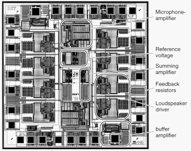
Fig. 2: Layout of the HST ASIC.
Conclusion
The development of an analogue ASIC helped the company to reduce the system costs, increase the reliability by implementing additional monitoring functions, and to a certain extent standardize their products. Prototyping services like those provided by EUROPRACTICE proved to be very valuable, their cost-effectiveness being an essential argument in easing the decision of an SME towards the use of new technologies. On the other hand, comparatively long turnaround times acceptable for universities may irritate industrial partners, and the consequences on project schedules have to be pointed out from the very beginning. In this sense both partners gained experience in managing projects including MPW prototyping.
References
[1] P.E. Allen and D.R. Holberg, CMOS Analog Circuit Design, Saunders College Publishing, 1987, p. 462.
[2] J.N. Babanezhad and R. Gregorian, "A Programmable Gain/Loss Circuit", IEEE J. Solid State Circuits, vol. SC-22, pp. 1082 – 1090, Dec. 1987.
[3] K.R. Laker and W.M.C. Sansen, "Design of analog integrated circuits", McGraw-Hill, 1994.
Project Information
Project Manager
Dipl.-Ing. Nikolaus Kerö
Institut für Allgemeine Elektrotechnik und Elektronik, TU Wien, A-1040 Vienna
Project Group
|
Last Name |
First Name |
Status |
Remarks |
|
Cadek |
Gerhard R. |
dissertation |
|
|
Kausel |
Wilfried |
dissertation |
|
|
Kerö |
Nikolaus |
dissertation |
|
|
Kowarsch |
Eduard |
technician |
|
|
Sauter |
Thilo |
dissertation |
|
|
Thorwartl |
Peter C. |
dissertation |
Doctor’s Theses
Cooperations