Single-Mode and Single-Beam Emission from Surface Emitting Laser Diodes Based on Surface Mode Emission
A. Köck, A. Golshani, R. Hainberger, P. O. Kellermann, E. Gornik
Institute of Solid State Electronics &
Center of Microstructure Research (MISZ), TU Wien,
A-1040 Vienna, Austria
L. Korte
Siemens AG, D-81730 München, Germany
Single-mode and single-beam emission has been achieved from surface emitting laser diodes based on the surface-mode-emission technique. By employing an optimized device design and a first-order grating coupler, the laser diodes show under pulsed operation condition a single-mode emission with a linewidth of 0.11 nm. A power up to 3.6 mW is emitted into a single, surface-emitted beam, which has a beam divergence of 0.20o.
The most important impact of laser diodes is the area of transmission systems for optical telecommunication, where single-longitudinal-mode (SLM) laser diodes are required to achieve a high transmission capacity and distance. Among the various types of single-mode laser diodes the distributed-Bragg-reflector (DBR) and the distributed-feedback (DFB) laser diodes are most commonly used and have been successfully employed in commercial transmission systems [1], [2]
By far most of the present SLM-laser diodes are conventional edge emitters, while many novel optoelectronic applications, like optical interconnects, optical computing and high power laser arrays, require surface emitting laser diodes. Various types of surface emitting laser diodes, like horizontal cavity lasers with 45°-mirrors, DBR and DFB-laser diodes with second order grating couplers, Master-Oscillator-Power-Amplifiers and Vertical Cavity Surface Emitting laser diodes have been developed so far [3] – [5].
We have presented a new concept based on the surface-mode-emission (SME) technique, which has been applied to realize a new type of surface emitting laser diode [6], [7]. In addition we have recently proposed this technique as flexible concept for a new type of SLM-laser diode [8]. A real single-mode emission from this type of laser diode, however, has not been achieved yet [9].
We report on a single-mode and single-beam emission achieved from SME-laser diodes. Under pulsed operation condition a single-mode emission with a linewidth of 0.11 nm is achieved, while a power up to 3.6 mW is emitted into a single, surface-emitted beam with a beam divergence of 0.20o. This has been achieved by an optimized device geometry and by fabricating high-quality first-order gratings with an Ion-milling etching technique.

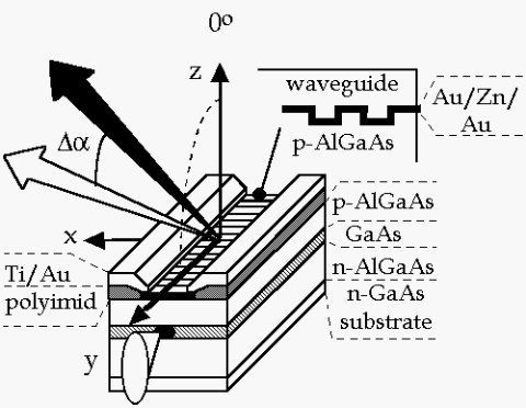
Fig. 1: Geometry of the SME-laser diodes. The surface grating is oriented in y-direction, while the laser stripe is oriented in x-direction. The window for the SME-coupling process has a width of 8 µm and extends over the whole length of the cavity.
The SME-technique is based on an interactive coupling between the laser light propagating in the active region of the laser diode and a transverse electrically polarized TE0-surface mode propagating in a waveguide structure on top of the laser diode. This requires a special device geometry, which is shown in Fig. 1. The laser diode is a conventional GaAs/AlGaAs-double-hetero-structure grown by MOCVD. An n-AlGaAs cladding layer (thickness 1300 nm, 35% Al) is grown on a n-GaAs substrate followed by an undoped GaAs active region (thickness 90 nm). Next is a p-AlGaAs cladding layer (thickness 550 nm, 30% Al) with a highly doped p-GaAs cap layer (thickness 5 nm) on top. While in recent structures p-AlGaAs cladding layers with thickness of 700 nm and 900 nm were used, the thickness has been reduced to 550 nm in order to achieve an enhanced coupling between the laser light and the TE0-surface mode. A first-order grating, which is holographically exposed in photoresist, is etched into the p-AlGaAs-top-cladding layer by ion-milling (grating period L = 415 nm, grating amplitude 100 nm). This etching technique has strongly improved the quality of the grating as compared to recent samples, where a wet-chemical etching process has been used. The evaporation of a semitransparent Au/Zn/Au metal stripe (50 Å/50 Å/200 Å) with a width of 12 µm oriented normal (x-direction) to the grating grooves (y-direction) defines the laser stripe. The single laser stripes are separated at a distance of 250 µm, the surface of the sample in between is isolated with polyimid. Ti-Au contact pads (500 Å/3000 Å), which overlap the laser stripe from both sides by 2 µm leaving a 8 µm wide window in the center of the laser stripe, are evaporated on the polyimid isolation. Next the laser stripe is spin-coated with photoresist (Hoechst AZ 6615, thickness 250 nm) forming a slab wave guide on top of the laser diode, which supports the TE0-surface mode. Finally the laser bars are cleaved to a length between 400 µm and 600 µm.
Locally in the window the laser light is coupled to the TE0-surface mode. In this experiment the window extends over the whole cavity length, while in recent experiments the window (length 200 – 300 µm) was only a part of the cavity length. This increases the coupling efficiency from the laser light to the surface mode. Part of the laser light is scattered from the active region via the surface grating into the waveguide. The light is propagating in the waveguide as a zig-zag-wave, where part of the zig-zag-wave is scattered into air into the emission angle a resulting in efficient surface emission. In addition, part of the zig-zag-wave is scattered back into the active region providing a positive, wavelength selective feedback process, which can result in a single-mode emission. These coupling mechanisms have been discussed in detail in Ref. [8].
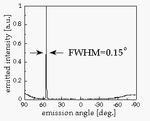
The corresponding far-field pattern in DC-operation is shown in Fig. 2. The farfield pattern is measured by scanning the laser diode along the laser stripe (x-direction) from one cleaved facet to the other. The sample emits the light into a single beam in an emission angle of -55.35o. The beam divergence in x-direction is less than 0.15o, while the beam divergence in the direction normal (y-direction) to the laser stripe is 8o. The intensity emitted per solid angle into the single beam is more than 15 times higher than the edge emitted intensity per solid angle, which demonstrates the high efficiency of the SME-technique. Presently a power up to 3.6 mW is emitted into the single beam, which is 15 % of the totally emitted power of 24 mW.

Fig. 2: The far-field pattern measured by scanning the laser diode along the laser stripe (x-direction) from one cleaved facet to the other. The SME-laser diode emits the light into a single beam in an emission angle of -55.35°. The beam divergence is less than 0.2o, a power up to 3.6 mW is emitted into this single, surface-emitted beam.
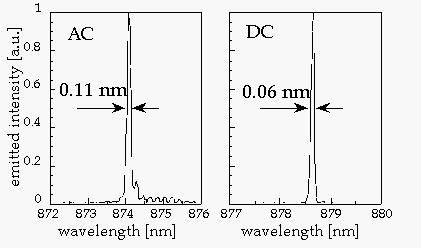
The SME-laser diodes show threshold current densities between 1.8 and 2 kA/cm2. The wavelength emission spectrum of a SME-laser diode (threshold current Ith = 140 mA) in pulsed biased condition (pulse width 0.6 µsec, f = 40 kHz) at a current of 1.3 x Ith is shown in Fig. 3 (left). The sample shows a single-mode emission at l = 874.08 nm with a full-width-half-maximum (FWHM) of 0.11 nm. The single-mode emission is maintained with increasing current, but the FWHM increases up to 0.17 nm at 1.6 x Ith and up to 0.27 nm at 1.8 x Ith. The right part of Fig. 3 shows the DC emission spectrum at a current of 205 mA. The laser diodes operates in a single-mode, the minimum linewidth achieved is 0.06 nm, the best side-mode-suppression-ratio is 24 dB.

Fig. 3: Single-mode emission spectrum of a SME-laser diode in AC-condition (left) (pulse width 0.6 µsek, f = 40 kHz) at a current of 180 mA (= 1.3 x Ith) and in DC-operation at a current of 205 mA (right).
Discussion and Conclusion
The main advantage of the SME-type of laser diode as compared to surface emitting DBR- or DFB-laser diodes is a simple and flexible fabrication process. It utilizes the well-established technique of the conventional striped laser and requires no regrowth. The present performance of the SME-type of laser diode (relatively high threshold current densities (1.8 – 2 kA/cm2), low output power) can be optimized by mirror-coatings: High-reflection mirrors on the cleaved facets will both decrease the threshold current density as well as increase the surface emitted power. The use of a quantum-well structure as active region instead of the double-hetero-structure should further decrease the threshold current density.
As has already been demonstrated [9], the emission wavelength (and so the emission angle) can be adjusted by the waveguide thickness and depends on the refractive index of the waveguide. This makes the SME-type of laser diode very suitable to be employed in practical applications: On one hand wavelength-division-multiplexing (WDM) techniques require on the transmitter side arrays of single-mode laser diodes, which emit at different, well-defined wavelengths. On the other hand WDM requires wavelength-tunable laser diodes on the receiver side for the heterodyne-detection-scheme [10]. The fabrication of laser bars containing laser diodes emitting at well-defined, different wavelengths (wavelength spacing Dl ~ 0.5 – 3 nm) can be realized by processing adjacent SME-laser diodes with slightly different waveguide thickness (Dd ~ 2 – 5 nm). The use of an electro-optically active polymer, for example, as waveguide material will allow a continuous change of the waveguide’s refractive index by applying an electric field across the waveguide. This would result in a continuous wavelength-tuning around a central wavelength primarily defined by the waveguide thickness. Thus SME-laser diodes have the potential to achieve both WDM-requirements. Therefore it is essential to apply the SME-technique to laser diodes operating in the 1.3 µm- and 1.5 µm-wavelength regime.
In addition due to their high beam quality, surface emitting SME-laser diodes can be employed as direct optical interconnects. For this specific application the steering of the surface emitted beam by tuning the emission wavelength is of high importance.
Acknowledgments
This work was also sponsored by the Stiftung Volkswagen, Hannover, Germany.
References
[1] J. Buus, "Single Frequency Semiconductor Lasers", Tutorial Texts in Optical Engineering, Vol. TT5, SPIE Optical Engineering Press (1991)
[2] T. Ikegama, in "Optoelectronic Technology and Lightwave Communications Systems", edited by C. Lin, Van Nostrand Reinhold, New York (1989)
[3] K. Iga and F. Koyama, in "Surface Emitting Semiconductor Lasers and Arrays", edited by G. A. Evans and J. M. Hammer, Academic Press, London (1993)
[4] D. Botez and D.R. Scifres, "Diode Laser Arrays", Cambridge University Press, New York (1994)
[5] N.W. Carlson, "Monolithic Diode-Laser-Arrays", Springer Verlag, Berlin, Heidelberg (1994)
[6] A. Köck, A. Seeberg, M. Rosenberger, E. Gornik, C. Thanner, L. Korte, Appl. Phys. Lett. 63, 1164 (1993)
[7] A. Köck, C. Gmachl, E. Gornik, M. Rosenberger, C. Thanner, and L. Korte, Appl. Phys. Lett. 64, 836 (1994)
[8] A. Köck, S. Freisleben, C. Gmachl, E. Gornik, M. Rosenberger, L. Korte, P. L. de Souza, Appl. Phys. Lett. 67, 452 (1995)
[9] A. Köck, A. Golshani, R. Hainberger, N. Finger, C. Gmachl, E. Gornik, L. Korte, Photonics West, OE/LASE’96, SPIE-Proceedings Vol. 2682, p. 169 (1996)
[10] J.E. Midwinter, Y.L. Guo, "Optoelectronics and Lightwave Technology", John Wiley & Sons, Chichester (1992)
Project Information
Project Manager
Dr. Anton Köck
Institut für Festkörperelektronik, Technische Universität Wien, A-1040 Vienna
Project Group
|
Last Name |
First Name |
Status |
Remarks |
|
Finger |
Norman |
dissertation |
|
|
Gianordoli |
Stfan |
student |
|
|
Golshani |
Amir |
dissertation |
|
|
Haider |
Manfred |
student |
|
|
Hainberger |
Rainer |
dissertation |
|
|
Kellermann |
Peer Oliver |
student |
|
|
Köck |
Anton |
assistent professor |
|
|
Maier |
Thomas |
dissertation |
|
|
Schrenk |
Werner |
student |
Publications in Reviewed Journals
Presentations
Doctor’s Theses
Cooperations