FTIR Measurements of the Hydrogen Concentration of SiN Layers
I. Jonak-Auer, R. Meisels, F. Kuchar
Institute of Physics, University of Leoben,
A-8700 Leoben, Austria
We report on new very accurate Fourier Transform Infrared (FTIR) measurements of the hydrogen content of amorphous silicon nitride (SiN) layers by evaluating the corresponding absorption lines with the help of polynomial fits. Our measurements show large differences in the hydrogen concentrations comparing layers which were deposited by plasma-enhanced chemical vapor deposition with layers deposited by thermal low-pressure chemical vapor deposition. The hydrogen content of the layers can be successfully reduced by applying various annealing procedures.
Amorphous SiN layers are essential for the semiconductor industry as an encapsulant for silicon integrated circuits, as a diffusion barrier for H2O and sodium ions [1], as passivation films, oxidation masks [2], gate insulators, and capacitor dielectrics [3]. Since the quality of SiN layers is highly dependent on the hydrogen content, the measurements we present are very important for the semiconductor industry. Hydrogen in SiN layers is chemically bound to Si and N, the source of hydrogen being the deposition reactants NH3, SiH4 and SiH2Cl2. If the hydrogen content in the layers is considerable, it will affect such properties as film structure, etch rate, stress and moisture permeability [4]. On the other hand, a certain amount of hydrogen in the films is desirable, because it reduces the trap density by passivating silicon dangling bonds which improves the device characteristics. Our measurements rely on the fact that the incoming IR radiation excites stretching vibrations of the Si-H and N-H bonds in the SiN layer, which leads to absorption lines in the MIR spectral region. The intensities of the absorption lines are directly related to the hydrogen content of the layer, thus providing a fast and non-destructive method of determining the hydrogen concentration. In this study we present a method of evaluating the N-H and Si-H absorption lines more accurately than it was possible up to now, we compare the hydrogen concentrations of SiN layers deposited by different processes and we also show how different annealing procedures influence the hydrogen concentration.
Our experiments were performed using a Bruker Fourier Transform Spectrometer IFS 113v with a Globar source, a KBr beamsplitter and a DTGS detector. In order to determine the areas of the absorbance peaks as accurately as possible we first measure a transmission spectrum of the sample (SiN layer + Si substrate). To correct the data for errors due to the absorption of the Si substrate itself we subtract a transmission spectrum of a pure Si wafer of the same thickness as the substrate of the coated wafer. From the resulting transmission spectrum the absorbance is calculated by:
absorbance = - log (transmission)
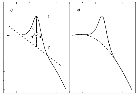
In contrast to commercially available FTIR software and recommended procedures in the literature [4], which in principle use linear baselines to evaluate the areas of the N-H and Si-H absorbance peaks at 3350 cm-1 and 2160 cm-1, respectively, we do a polynomial fit of the spectral background outside the absorption lines. This yields a much higher accuracy in determining the areas of the absorbance peaks and therefore the hydrogen concentration. Both cases are illustrated in Fig. 1, which shows a Si-H absorbance line evaluated with the linear baseline method (a) and with a polynomial fit (b). While for the linear baseline method the areas are simply approximated by (I-I’)·Dn, we determine the areas between the absorbance line and the polynomial fit by integration. Comparisons between the two methods of evaluation yield differences of up to 30%.
Fig. 1: a) Determination of absorbance area with the linear baseline method.
b) Determination of absorbance area with a polynomial fit.
In Fig. 2 the polynomial fit of Fig. 1 (b) is subtracted from the absorbance curve. The resultant line shape can very well be fitted by a Gaussian curve (dashed line), a fact which proves the high quality of the background fit.
SiN layers prepared both by plasma-enhanced chemical vapor deposition (PECVD) and thermal low-pressure chemical vapor deposition (LPCVD) with thicknesses between 1.5 µm and 10 nm were studied. For the thermally deposited SiN layers we also studied the influence of oxygen and nitrogen annealing procedures on the hydrogen concentration. Especially for the thinner thermal layers high intensity-resolution and stability of the measurement are essential since typical absorbance values correspond to changes in transmission of down to only 0.01%. Since absorptions due to CO2 and water-vapor in the air also occur in the same spectral regions as the Si-H and N-H absorption lines, thorough evacuation of the spectrometer is essential for obtaining correct results.
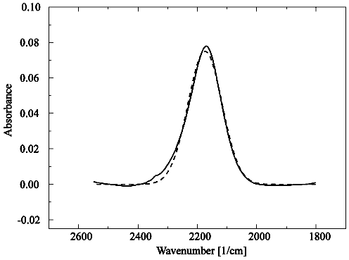
Fig. 2: Polynomial fit subtracted from absorbance curve (solid line) and appropriate Gaussian fit (dashed line).
In order to quantitatively determine the hydrogen concentration of SiN layers by FTIR it is necessary to have calibration factors which allow the conversion between the intensity of the absorption lines and the hydrogen concentration. One method of quantitative hydrogen concentration determination [4] is the resonant nuclear reaction
H + 15N ® 12C + 4He + g.
A beam of accelerated 15N++ ions impinges upon the SiN film and penetrates completely through to the Si substrate. There is appreciable probability for reaction only at the precise energy of 6.385 MeV. Thus, if the sample is bombarded with ions at this energy, the number of g rays measured to come from the sample is proportional to the hydrogen concentration at the film surface. By increasing the energy of the ions a concentration profile of hydrogen versus depth can be determined and therefore the total hydrogen concentration can be measured. The total hydrogen concentration must then be apportioned properly between the Si-H and N-H bands which show different absorptivities (absorption per bond). The resulting equations, which relate the number of N-H and Si-H bonds per cm2 to the areas of the N-H and Si-H absorbance lines, respectively, are [5]:
![]()
Conclusion
The total hydrogen concentration in our PECVD layers varies between 1.3·1022 and 2.0·1022 cm-3, whereas the hydrogen concentration in the thermal LPCVD layers is much smaller and lies between 4.5·1020 and 5.5·1021 cm-3. In PECVD layers the number of N-H bonds per cm3 varies between 5.9·1021 and 7.6·1021, while the number of Si-H bonds per cm3 is higher, namely between 5.8·1021 and 1.4·1022 .Thermal LPCVD layers on the other hand contain more N-H bonds than Si-H bonds: the number of N-H bonds per cm3 varies between 4.5·1020 and 5.8·1021, the number of Si-H bonds is approximately an order of magnitude smaller than that of N-H bonds, but the Si-H lines are too weak to allow a reliable quantitative evaluation. The effects of different annealing procedures of thermal LPCVD layers on the hydrogen concentration are shown in Fig. 3: Oxygen annealing reduces the hydrogen concentration more than nitrogen annealing, the hydrogen concentration decreases from 5.9·1021 cm-3 for the untreated layer to 1.0·1021 cm-3 for the nitrogen annealed layer to 4.5·1020 cm-3 for the oxygen annealed layer. With the presented FTIR method hydrogen concentrations of down to approximately 2·1020 cm-3 can be measured if the layer thickness is about 100 nm. For very thin layers of the order of 10 nm the detection limit is somewhat higher and lies at approximately 1·1021 cm-3.
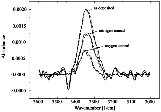
Fig. 3: Dependence of N-H absorbance lines (polynomial fits are already subtracted) on different annealing procedures for three samples (solid lines) and appropriate Gaussian fits (dashed lines).
Acknowledgments
Financial support for this work came from the Steiermärkische Wissenschafts- und Forschungslandesfonds, GZ AAW-12Ku24-93. All samples were prepared by Austria Mikro Systeme International AG.
References
[1] T.L. Chu: "Dielectric Materials in Semiconductor Devices", J. Vac. Sci. Technol., Vol. 6, 1970, pp. 25 – 33.
[2] C.R.M. Grovenor, Microelectronic Materials, IOP Publishing Ltd., 1989, ISBN 0-85274-270-3.
[3] M. Ino, N. Inoue and M. Yoshimaru: "Silicon Nitride Thin-Film Deposition by LPCVD with In Situ Vapor Cleaning and its Application to Stacked DRAM Capacitor Fabrication", IEEE Transaction on Electron Devices, Vol 41, 1994, pp. 703 – 708.)
[4] W.A. Lanford and M.J. Rand: "The hydrogen content of plasma-deposited silicon nitride", J. Electrochem. Soc., Vol. 49, 1978, pp. 2473 – 2477.
[5] W.R. Knolle: "Characterization of Plasma-Deposited SiN", Report AT&T Bell Laboratories, Reading Pennsylvania 19607, unpublished.
Project Information
Project Manager
Univ.-Prof. Dr. Friedemar Kuchar
Institut für Physik, Montanuniversität Leoben, A-8700 Leoben
Project Group
|
Last Name |
First Name |
Status |
Remarks |
|
Gold |
Herbert |
dissertation |
|
|
Jonak-Auer |
Ingrid |
dissertation |
|
|
Kuchar |
Friedemar |
university professor |
|
|
Lutz |
Josef |
assistant professor |
Publications in Reviewed Journals
Presentations
Doctor’s Theses
Cooperations