Ge+ Implantation into Silicon: Behavior of Deep Level Defects
L. Palmetshofer and Y. Suprun-Belevich
Institut für Halbleiterphysik, Johannes Kepler Universität Linz
A-4040 Linz, Austria
Implantation-induced defects and their annealing behavior in Si and SiGe have been investigated using deep-level transient spectroscopy. For Ge+ implantation in silicon three types of defects have been observed: vacancy-related defects which anneal out during annealing up to 600 °C, Ge-related defects which are formed during annealing and disappear at 900 °C, and radiation defects which are generated during annealing and disappear also at 900 °C. For ion bombardment of strained SiGe layers we found a strong influence of the strain on the production, diffusion and annealing of implantation-induced defects.
Introduction
Strained Si/SiGe layers can be used to improve the performance of silicon based electronic devices such as heterobipolar transistors and modulation-doped field effect transistors [1]. The Si/SiGe heterostructures are usually grown on Si substrates by molecular beam epitaxy at relatively low temperatures (< 750 °C). However, during the fabrication of a device, a number of ion implantation and high temperature annealing steps would typically follow the epitaxial growth. These processing steps are known to introduce defects or to modify already existing defects and can cause strain relief in the strained layers. At present, the properties of implantation-induced defects and their high-temperature annealing behavior in SiGe layers remain largely unstudied. Implantation-induced defects are also important in the case of ion-beam-synthesized SiGe layers. It has been shown that simple SiGe/Si heterostructures can be fabricated by ion implantation and solid-phase epitaxial regrowth [2].
In the context of these problems, a program was started to investigate implantation induced defects and their annealing behavior by deep-level transient spectroscopy (DLTS). Two aspects have been treated so far. First, the formation and annealing behavior of deep level defects after implantation of Ge+ into Si, and second, the influence of the mechanical strain on radiation defects.
Experimental
Phosphorus-doped CZ-grown Si wafers were implanted with 320 or 640 keV Ge+ ions with doses up to 3x1016 cm-2 corresponding to a peak Ge concentration of about 3 at.%. Deep level defects were investigated after subsequent isochronal annealing steps in the temperature range 100 – 1100 °C. Rapid thermal annealing (RTA) of the samples was performed by halogen lamp irradiation with 20 s exposure in a nitrogen gas flow. Deep-level transient spectroscopy measurements [3] were carried out using a 1 MHz capacitance bridge, a pulse generator and a liquid-nitrogen-cooled cryostat (77 – 400 K). The DLTS signal was obtained from the capacitance transient using the lock-in averaging method. Depth profiles of defects were obtained in double-pulse differential mode (DDLTS) [4].
Due to a 4% difference between the covalent radii of Si and Ge atoms the implantation of Ge into Si allowed us to vary the magnitude of the elastic misfit stress. The mechanical strain was investigated by high-resolution x-ray diffraction measurements using a four-crystal monochromator [5]. Some of the strained Ge+ implanted samples (in the following designated as Si:Ge) were then irradiated with 24 or 70 keV H+ ions at doses between 1x10¹⁰ and 1x1012 cm-2 to introduce radiation defects. The H+ implantation energy was chosen such that the radiation defects were placed into the region of the maximum gradient of the Ge concentration. All the ion ranges were calculated with the TRIM code [6]. The radiation defects formed by H+ irradiation were electrically characterized again by DLTS measurements.
Results and discussion
Deep level defects in Ge+ implanted Si
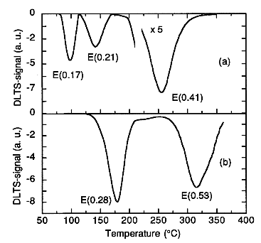
Three groups of deep levels have been observed by DLTS in the implanted samples. The first group of defects is observed in as-implanted samples and in samples annealed at low temperatures. Figure 1(a) shows a typical DLTS spectrum of Si implanted with a low dose of Ge+. The defects are labeled according to their energy position in the gap in eV. Three defects are detected in such samples: E(0.17), E(0.22) and E(0.41). Annealing experiments show that these defect levels are observed up to about 600 °C annealing temperature. The concentration of the defects decreases continuously with the annealing temperature.
Fig. 1: DLTS spectra of Ge+ implanted Si (640 keV): (a) dose 1011 cm-2, annealing at 100°C; (b) dose 1012 cm-2, annealing at 700 °C.
The second group of defect levels is observed after high temperature annealing. Figure 1(b) shows a typical DLTS spectrum of Ge+ implanted Si after annealing at 700°C. Two new defect levels, E(0.28) and E(0.53), are observed instead of those in as-implanted silicon. The new levels show up at about 500 °C and disappear only after annealing at very high temperatures (> 900 °C). In samples implanted at doses above 1013 cm-2 an additional minority carrier trap E(+0.17) is observed after 700 °C annealing, which disappears also above 900 °C. The third group of defect levels — two less dominant levels at E(0.40) and E(0.15) — is also observed after high temperature annealing between 700 and 900 °C.
The three levels observed in as-implanted silicon can be attributed to vacancy-related defects: E(0.17): vacancy-oxygen pair, E(0.21): divacancy, and E(0.41): a mixture of the divacancy and the phosphorus-vacancy pair [7]. The position and shape of the defect profiles measured by DDLTS coincides very well with the vacancy distribution calculated by the TRIM code. The profiles are shifted towards the surface as compared with the ion distribution.
The levels E(0.28) and E(0.53) observed in the temperature region 500 – 900 °C can be attributed to defect complexes containing Ge atoms. The position and shape of the profiles of these levels coincide with the profile of the ion distribution according to TRIM. The Ge-related levels are not formed during ion implantation, they are created during the annealing as a result of the recrystallization of amorphous inclusions and the release of Ge atoms from them. This process is accompanied by a sharp decrease of the defect-related mechanical strain.
The levels E(0.15) and E(0.40) observed after high temperature annealing are not related to the implanted species. From the shape of the defect profiles and from the fact that similar levels were observed also in Si+ implanted silicon it is concluded that the levels are related to radiation defects. The defects are generated during the recrystallization of amorphous inclusions and are not observed after implantation at doses above 1013 cm-2.
The main message of our study of deep levels in Ge+ implanted silicon together with strain measurements for the SiGe technology is that it is possible to obtain SiGe layers after implantation of Ge+ into silicon and appropriate annealing. The radiation defects can be annealed out completely and the Ge atoms are introduced on regular lattice sites. So far experiments have been performed only with low Ge concentrations (up to 3 at%). Since for doses above the amorphization dose (about 1014 cm-2) the annealing of the radiation defects occurs by solid state epitaxial regrowth, higher Ge concentrations are not expected to cause difficulties.
Influence of mechanical strain on radiation defects
The response to ion implantation is different for a strained SiGe layer and unstrained silicon. This has been found by investigating radiation defects after bombardment with H+ ions. H+ bombardment of Si introduces the vacancy-related defect levels E(0.17). E(0.21) and E(0.41) as described above, and in addition, a H-related level E(0.30) [7].
The production rates of these defects are essentially lower in strained Si:Ge samples. The decrease of the defect concentrations in Si:Ge as a function of the stress is shown in Fig. 2. The concentration of the defects was obtained from DLTS and DDLTS measurements, the stress was calculated from the strain in the implanted layer measured by x-ray diffraction [8]. DDLTS measurements have shown that defect profiles are significantly broader in Si:Ge samples than in silicon. The annealing behavior of the deep levels is also different for Si and Si:Ge. The annealing of the vacancy-related defects generally takes place in two stages. In the Si:Ge samples the beginning of both stages is shifted towards lower temperatures. The onset for the annealing of the H-related level E(0.30) is also shifted to lower temperatures in the Si:Ge samples.
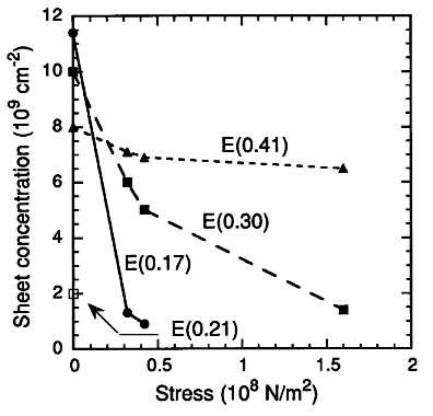
Fig. 2: Concentration of the defects in Si:Ge introduced by H+ bombardment (70 keV, 5x1010 cm-2) versus the Ge-related stress calculated from the measured strain. Stress zero denotes the Si reference sample.
The behavior of the radiation defects in Si:Ge cannot be explained by changes in the primary defect production (vacancies and interstitials) during bombardment due to the slightly changed stoichiometry. It is concluded that the Ge-related misfit strain is responsible for the reduced production rates of the observed defects, broadening of the defect profiles and the shift of the annealing stages. The production of primary defects (vacancies and interstitials) during ion bombardment and their behavior afterwards (diffusion, annihilation, capture by impurities, etc.) takes place in a field of mechanical stress. Elastic energy can be transferred to primary defects, thus influencing their behavior and the formation of defect complexes observed by DLTS. A detailed discussion is given in refs. [8] and [9].
References
[1] F. Schäffler: in "Grundlagen und Technologie elektronischer Bauelemente", (Gesellschaft für Mikroelektronik,Wien, 1995), p. 93.
[2] F. Corni, S. Frabboni, G. Ottaviani, G. Queirolo, D. Bisero, C. Bresolin, R. Fabbri, M. Servidori: J. Appl. Phys. 71 (1992) 2644.
[3] D.V. Lang: J. Appl. Phys. 45 (1974) 3023.
[4] H. Lefevre, M. Schulz: Appl. Phys. 12 (1977) 45.
[5] A. Pesek, P. Kastler, K. Lischka, L. Palmetshofer: Nucl. Instr. Meth. B 80/81 (1993) 569.
[6] J.F. Ziegler, J.P. Biersack, U. Littmark: "The Stopping and Range of Ions in Solids", Vol. 1 (Pergamon, New York, 1985).
[7] L. Palmetshofer, J. Reisinger: J. Appl. Phys. 72 (1992) 2167.
[8] Y. Suprun-Belevich, L. Palmetshofer: Nucl. Instr. Meth. B 115 (1996) 557.
[9] Y. Suprun-Belevich, L. Palmetshofer: Nucl. Instr. Meth. B, accepted.
Project Information
Project Manager
Univ.-Doz. Dr. Leopold Palmetshofer
Institut für Halbleiterphysik, Johannes Kepler Universität Linz, A-4040 Linz
Project Group
|
Last Name |
First Name |
Status |
Remarks |
|
Ablinger |
Karlheinz |
technician |
|
|
Palmetshofer |
Leopold |
associate professor |
|
|
Schmidt |
Thomas |
dissertation |
|
|
Suprun-Belevich |
Yuri |
postdoc |
University Minsk |
|
Wirtl |
Elisabeth |
technician |
50% GMe funding |
Publications in Reviewed Journals
Presentations
Doctor’s Theses
Cooperations