Pattern Transfer of Nanostructures
G. Stangl, P. Hudek, P. Hrkut, K. Riedling, W. Fallmann
Institut für Allgemeine Elektrotechnik und Elektronik,
TU Wien, A-1040 Vienna, Austria
The target of the investigations reported here was the patterning of relatively thick layers of sputtered carbon down to sub-µm structures by means of anisotropic reactive ion plasma etching. A process could be successfully developed which permits the preparation of carbon structures with an aspect ratio in excess of 1:4, using a thin poly-silicon layer as an etching mask.
An obvious etching agent for carbon layers is oxygen plasma since the reaction products are gaseous and volatile; no re-deposition of etched material may therefore occur. However, conventional resist materials are subject to an etch rate in oxygen plasma that is by far greater than the etch rate of a dense carbon film. This prevents the preparation of structures with a high aspect ratio because it would require a resist thickness that significantly exceeds the thickness of the carbon film and therefore impedes the preparation of narrow lines. Hence, it is necessary to use a masking material for the etching process that is not or not significantly affected by the oxygen plasma.
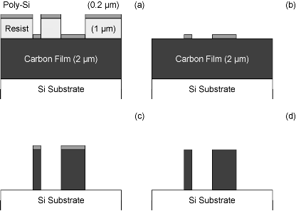
An attractive candidate for such a masking material is poly-silicon. Although it is also oxidized by the oxygen plasma its masking properties do not deteriorate due to the oxidation because the oxygen plasma hardly attacks silicon dioxide. Patterning by reactive ion etching a thick carbon film down to sub-µm dimensions requires therefore a three-step approach: (1) Deposition of a poly-silicon layer atop of the carbon film; (2) structuring of the poly-silicon layer by a suitable lithographic process; and (3) transfer of the structures in the poly-silicon layer into the carbon film by reactive ion etching.
Experimental
The carbon films that were subjected to our etching experiments were generally very dense, electrically well conducting layers with thicknesses of 1 – 2 µm; they were prepared by means of RF sputtering at the Academy of Sciences in Bratislava. Conventional silicon wafers served as substrates. The poly-silicon etching mask film was also deposited by RF sputtering; a thickness of 0.2 µm proved to be sufficient for withstanding the etching of a 2 µm carbon layer. The poly-silicon mask was structured with a lift-off technique; the resist patterns were defined by E-beam lithography. The subsequent carbon etching took place in a Perkin-Elmer ECR-RIE-4000 plasma etcher at the Institut für Allgemeine Elektrotechnik und Elektronik in Vienna, using pure oxygen as an etching agent. In some experiments, the poly-silicon mask layer was subsequently removed in the same vacuum process by etching with CF4 + SF6 (Fig. 1).
Fig. 1: Structuring of carbon films: (a) after deposition of the poly-Si mask layer; (b) after lift-off; (c) after anisotropic RIE-etching of the carbon film; (d) after removal of the poly-Si mask layer.
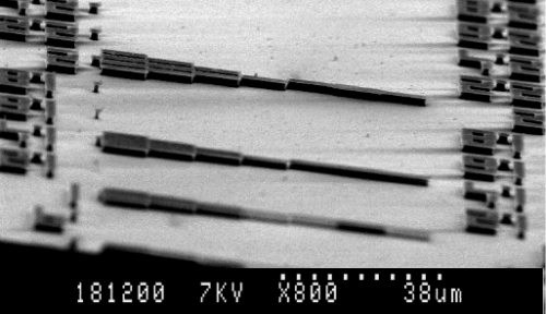
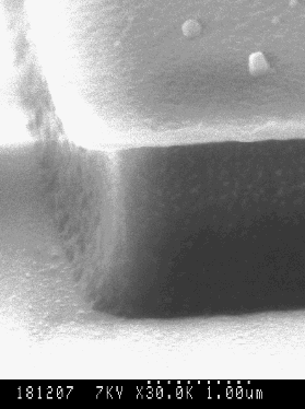
Fig. 2: Etched carbon structures on a silicon substrate.
By a proper choice of the process parameters, very steep sidewalls of the carbon structures could be obtained, with only a slight intentional underetching whose extent could be adjusted with the process parameters (Figs. 2 and 3).
|
|
|
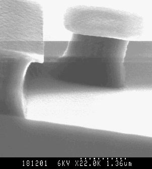
Fig. 3: Etched carbon structures with the poly-Si mask layer still on top.
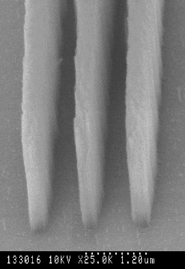
Further optimization of the process permitted the preparation of structures with an exceedingly high aspect ratio, virtually vertical sidewalls, and a lateral resolution down to 0.2 µm or less (Fig. 4).
|
|
|
Fig. 4: High aspect ratio carbon structures after the removal of the poly-Si mask layer.
Conclusion
Our investigations show that sputtered carbon layers with thicknesses of several micrometers may be patterned down to a few tenths of a micrometer by reactive ion etching using a poly-silicon etching mask. The ratio between anisotropic and isotropic etching can be varied over a broad range by a variation of the process parameters. It is therefore possible to obtain a practically totally anisotropic etching behavior and very steep structures with an aspect ratio of up to 1:20. This permits the preparation of sub-µm carbon structures for a variety of electronic and micromechanical devices.
It should be noted that the deposition of the carbon films is crucial for the entire process: Special sputtering techniques are required to reduce the stress in the deposited layers that otherwise would lead to fractured edges of the etched structures and to the formation of residues where the film ought to be removed. Without stress reducing processing, such effects occur at or above a carbon film thickness of 1 µm. The deposition process developed at the Academy of Sciences in Bratislava currently guarantees stress-free deposition of 4 µm thick carbon films; it is planned to extend the feasible carbon film thickness range to 10 µm.
Acknowledgments
In addition to the Society for Microelectronics, the Ost-West-Fonds (project OWP 92) financially contributed to this work.
Project Manager
Univ.-Doz. Dr. Karl Riedling
Institut für Allgemeine Elektrotechnik und Elektronik, TU Wien, A-1040 Vienna
Project Group
|
Last Name |
First Name |
Status |
Remarks |
|
Fallmann |
Wolfgang |
university professor |
|
|
Riedling |
Karl |
associate professor |
|
|
Schalko |
Johannes |
dissertation |
partial GMe funding |
|
Stangl |
Günther |
technician |
Publications in Reviewed Journals
Presentations
Doctor’s Theses
Cooperations