Microstructure Research: Cleanroom Vienna
E. Gornik, G. Strasser
Institute of Solid State Electronics &
Center of Microstructure Research (MISZ), TU Wien,
A-1040 Vienna, Austria
In this paper, the main activities in the cleanroom of the MISZ are described. The cleanroom of the MISZ was opened 1993; during 1994, most of the equipment for the production of semiconductor devices was installed. Since 1995, state of the art growth of III-V compounds as well as the production of patterned masks used in lithography is done on a regular basis. One of the main research areas of our institute is the preparation and characterization of III-V devices. Therefore the fke maintains several collaborations with national and international research institutions and companies by providing them with epitaxial layers (III-V-compounds). A second main research topic is the production of micron and sub-micron devices down to nanometer scale. Patterned masks for optical lithography are also provided to different institutions.
Introduction
Since 1995, the cleanroom of the MISZ is operated and maintained on a regular basis. Main research areas are the state of the art growth of III-V compounds and the processing of these layers resulting in transport and optical devices. Processing steps are lithography, structuring (different etching techniques), planarization, and metallization of the different layers. A production of patterned masks is part of the cleanroom facility as well as the deposition of dielectric material by chemical vapor deposition. Supplementary to the normal operation and maintenance of the cleanroom and the cleanroom equipment, additional equipment was installed. Testing of the cleanroom quality and adjustment (laminar air flow, filters, cooling, humidity…) if necessary is done periodically.
During 1996, various new equipment was installed in the cleanroom of the MISZ. In detail, an Oxford Plasmalab 80+ system was installed in a two chamber master-slave configuration. One chamber is equipped for RIE processes, the second chamber is a plasma CVD system.
The RIE system has two main applications in the MISZ: First, almost all grating couplers for the GaAs-AlGaAs surface emitting lasers are fabricated on this machine. Second, all samples fabricated by electron beam lithography are processed in this machine. As a first result, a single quantum dot was fabricated on a high mesa, which was subsequently used as tip on a scanning tunneling microscope.
The CVD machine is used for the deposition of insulating Si-nitride and Si-oxide films. Insulating layers are necessary for the fabrication of multi layer device structures, such as the 3-terminal devices for ballistic electron spectroscopy and also for MOS-device structures. Furthermore, dielectric laser mirrors are fabricated with this machine.
As second major installation, a Süß MJB3 UV mask aligner was brought into the cleanroom. The main purpose of this machine is to guarantee an industrial standard in optical lithography. The new mask aligner is capable to transfer patterns down to 0.5 µm, which is the limit of our CGA machine for mask fabrication. The new mask aligner is used for GaAs lasers with surface grating couplers and also for the fabrication of sub-µm tunneling diodes and the 3- and 4-terminal devices used in ballistic electron spectroscopy.
Research Activities
Reactive Ion Etching
A new type of surface-emitting laser diode has been developed, which is based on a Surface-Mode-Emission-(SME)-technique. This technique utilizes an interactive coupling process between the laser mode propagating in the cavity and a TE0-surface mode in a waveguide structure on top of the laser diode. This technique has been successfully applied to GaAs/AlGaAs-laser diodes to achieve a single-mode emission and a single, surface emitted beam with a beam divergence as low as 0.15°. Presently a power up to 4 mW (which is 20 % of the total emitted power) is emitted into the single beam.
Usually laser diodes are cleaved to single devices out of the chip. For the fabrication of 2-dimensional arrays of laser diodes, which is of high importance for coherent high-power application, the mirror facets have to be etched by a proper etching technique. High-reflecting coatings on the etched mirrors suppress the edge emission of SME-laser diodes and should therefore result in a strongly increased surface emission.
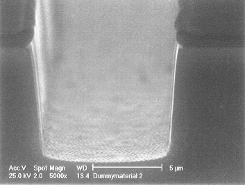
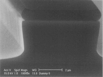
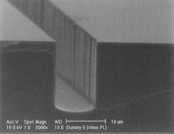
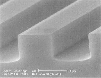
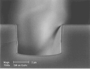
Laser mirrors make high demands on the etching technique. The etched facets have to be perfectly vertical and the roughness has to be less than l/(10 . nGaAs), which requires at an emission wavelength of 880 nm a smoothness of less than 20 nm. As a wet-chemical etching process is not suitable to achieve vertical facets, a Reactive-Ion-Etching-(RIE)-technique has been used. Photoresist, metal and dielectric layers of SiO and SiN were used as etching masks. The best results have been achieved with photoresist-masks removable by a solvent instead of etchants necessary for metal- and dielectric-masks, which can corrode the GaAs/AlGaAs-samples. SiCl4 was used as etching gas. The angle of the etched sidewalls depends strongly on the etching parameters and can be adjusted via the pressure and the RF-power. The etching results have been controlled with help of a Dektak-profiler and the SEM-system. Figure 1 shows a SEM-photograph of an etching facet achieved in a GaAs-sample at a pressure of 100 mTorr and a power of 150 W (SiCl4-flow 15 sccm, duration 10 min, self bias 300 V). The sidewalls are only a few degrees off the vertical. Figure 2 shows a result achieved at a pressure of 4 mTorr and a power of 100 W (SiCl4-flow 15 sccm, duration 7 min, self bias 500 V). Here the sidewalls are even overhanging, while Fig. 3 shows a result achieved at a pressure of 50 mTorr and a power of 75 W (SiCl4-flow 15 sccm, duration 30 min, self bias 250 V), where the sidewalls are vertical. The slight roughness in longitudinal direction is due to the photomask used for the exposure. Figure 4 finally shows a perfect result with roughness less than 10 nm.
|
|
|
|
Fig. 1: SEM photograph of RIE etched GaAs (Photoresist not removed) |
Fig. 2: SEM photograph of RIE etched GaAs (Photoresist not removed) |
|
|
|
|
Fig. 3: SEM photograph of RIE etched GaAs (Photoresist removed) |
Fig. 4: SEM photograph of RIE etched GaAs (Photoresist removed) |
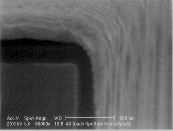
Finally the vertical mirror facets have been coated with SiN and Au. SiN has been deposited by a PECVD-process, Fig. 5 shows a SiN-coating on GaAs, which has been deposited at a RF-power of 10 W, a pressure of 1 Torr at a background pressure of 25 mW, a substrate-temperature of 200 °C. The SiH4- and NH3-gas flows are 700 sccm and 18 sccm. The deposition rate is typically 13 nm/min. The final result of a high-reflecting SiN/Au-coating on a vertical laser mirror is shown in Fig. 6. The thickness of the SiN- and the Au-layer is 180 nm and 140 nm, respectively. The apparent thickness fluctuation in the Au-film thickness is due to the cleavage necessary for the SEM-inspection.
First InGaAs/GaAs-laser diodes fabricated with RIE-etching and mirror coatings show threshold-current densities of 1.5 kA/cm2, which are close to the values achieved for a cleaved device. This demonstrates the excellent quality of the etching process and the subsequent deposition technique of the mirror-coatings.
|
|
|
|
Fig. 5: SEM photograph of SiN-coating on GaAs |
Fig. 6: SEM photograph of SiN/Au-coating on GaAs |
Growth of III-V Materials
Since 1995 growth of epitaxial GaAs material and related compounds is done in the MISZ with a molecular beam epitaxy system (GEN II). A modular GEN II solid source MBE machine is a system specially designed for high quality growth of III-V materials. The controlled growth of single crystalline layers on an atomic scale makes it possible to design new materials with optimized electrical and optical characteristics.
A carbon dopant source was installed in the epitaxy system giving the possibility to grow p-type material with very low diffusion length of the dopant material and therefore very abrupt doping profiles.
Growth and Characterization of Modulation Doped High Mobility 2DEGs (G. Strasser, J. Smoliner, C. Eder, G. Ploner, L. Hvozdara)
Epitaxial growth of AlxGa1-xAs on GaAs gives a band discontinuity in the conduction and valence band. Intentional doping influences the Fermi levels and increases the band offset at the interface. Electrons move from the n-doped AlxGa1-xAs into the non-doped GaAs and form a two dimensional electron gas (2DEG). The offset and the bending of the bands prohibit the recombination of the carriers with the ionized impurities in the AlxGa1-xAs. Impurity scattering is the most dominant scattering mechanism at low temperatures. In a 2DEG this scattering process is drastically reduced due to the separation of carriers and impurities ("remote impurities"). This leads to electron mobilities up to 107 cm2/Vs (4.2 K).
Two-dimensional electron gases (GaAs/AlGaAs heterostructures) were grown with mobilities up to 1.8·106 cm2/Vs at 4 K and 3.5·106 cm2/Vs after exposure to red light. The sheet carrier concentrations vary from 0.5 to 5·1011 cm-2. Characterization was done via temperature dependent hall measurements (4 K to 300 K), SdH measurements, and cyclotron resonance absorption. Additional confinement by structuring and etching leads to quantum wire and quantum dot regimes. The optical and transport behavior of these low dimensional systems is investigated.
Design, Growth and Characterization of RTDs and SLs (G. Strasser, C. Rauch, K. Unterrainer, W. Heiß, L. Hvozdara)
The first working "three terminal devices" with electron injectors, drift regions and a "filter" to separate ballistic from thermal carriers were realized in December 1995. By the end of 1996 a big technological step further on was established by the first "four terminal device". Parallel to these activities, superlattice structures (GaAs/AlGaAs-superlattices with periods from 2 to 20 monolayers) were grown to investigate the doping behavior. Broken gap miniband structures and quantum cascade laser structures are designed, grown and measured. Aim of this work is the realization of terahertz detectors and emitters and the realization of an unipolar semiconductor laser in the infrared region. For a more detailed discussion of these projects see chapter 3.
Design, Growth and Characterization of Epitaxial AlGaAs Bragg Mirrors (G. Strasser, T. Maier
)
The MBE-growth of AlGaAs Bragg mirrors was optimized to an extent that enables us to grow these mirrors with maximum reflectivity at a desired wavelength. The reflectivity of the mirrors was measured with a precision of 1% and compared to a theoretical model containing the thicknesses of the layers as input-parameters (Fig 7). From this comparison, the deviation of the thicknesses from the nominal values could be determined and a calibration performed. Bragg mirrors grown with this calibration show good agreement with the theoretical model (calculated with nominal thicknesses) and exhibit maximum reflectivity at the wavelength they were designed for.
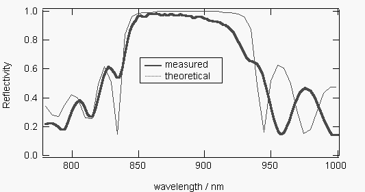
Fig. 7: Reflectivity vs. wavelength of a Bragg mirror consisting of 20 pairs Al0.1Ga0.9As/AlAs, designed for 880 nm.
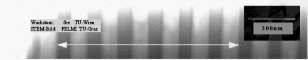
Fig. 8: TEM picture of AlAs/GaAs Bragg mirror (average thickness AlAs/GaAs: 133 nm)
Summary
In this summary a short description of running projects of the institute of solid state electronics (fke) are depicted which are not directly involved in the growth of semiconductor materials, but rely on III-V based samples and/or use devices patterned in the cleanroom (by optical, laser- or electron-beam lithography).
Fabrication, Characterization and Lithographic Structuring of Dielectric Bragg Mirrors (T. Maier)
Dielectric Bragg-mirrors for vertical-cavity surface emitting laser diodes offer an attractive alternative to MBE grown mirrors, allowing a greater flexibility to optimize important features of the laser such as threshold current, optical power and lasing wavelength by adjusting the mirror reflectivity and the resonator length to the MBE-grown structure.
We fabricated SiOx/SiNx-Bragg mirrors using PECVD and measured the spectral dependence of their reflectivity. The deposition was found to be very homogenous and highly reproducible, allowing the fabrication of tailor-made Bragg mirrors for a given wavelength. High-reflectivity mirrors (R > 0.98) were realized by deposition of 10 SiOx/SiNx-pairs (Fig. 9).
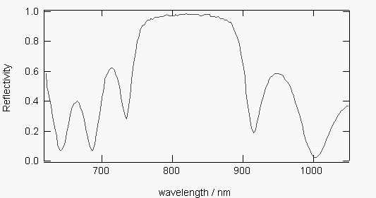
Fig. 9: Reflectivity vs. wavelength of 10 pairs SiOx/SiNx.
The SiOx/SiNx-layers were then patterned using standard photoresist masks. Etching was done in two steps: first by argon ion-milling, then in an SF6-plasma for which the substrate (GaAs) serves as an etch stop layer, leaving SiOx/SiNx mesas on a clean GaAs-surface.
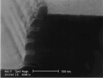
Fig. 10: SEM picture of a SiOx/ SiNx mesa (5 pairs)
Nanostructured Airbridges for THz Schottky Diodes (M. Hauser, E. Zottl, G. Strasser)
A new application of electron beam lithography (EBL) was the production of nanostructured metal airbridges, which are used to form ultrafast THz Schottky diodes. These devices operate at room temperature and can be used as detectors for far infrared radiation (FIR) or mixers for THz signals. New processes have been developed to reach the low capacitances necessary for diodes operating in the THz regime.
The diodes consist of n doped GaAs layers grown on a semiinsulating GaAs wafer. The diode is defined by proton implantation of the surrounding area. Therefore a mask covering only the active diode area is employed. It consists of a three layer stack of silicon nitride as a protective layer for the active diode area, a polyimide layer, and a thick layer of gold for masking of the implantation ions (Fig. 11).
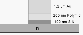
Fig. 11: Sketch of the ion implantation mask
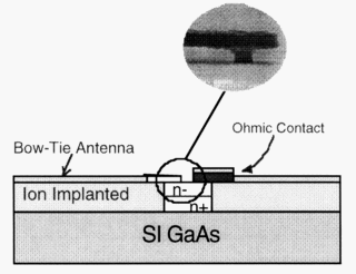
Fig. 12: Submicrometer Schottky diode design
A bowtie antenna is used to couple the FIR to the leads of the diode (Fig. 12). One lead connects the bowtie to the n-layer by an annealed ohmic contact. The Schottky contact forming the diode consists of a gold air bridge connecting the other end of the bowtie to the active diode area across the implanted region. A scanning electron microscope picture of this part of the device is shown in the insert. The airbridge is about 10 µm long, 200 nm wide and forms a Schottky contact with a diameter of less than 100 nm. The distance from the airbridge to the surface is about 250 nm. The capacitances of the leads are low enough to guarantee a cutoff frequency of more than 5 THz.
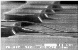
Fig. 13: SEM picture: airbridges.
BEEM Experiments on Quantum Wires (C. Eder, J. Smoliner)
In this project, a special scanning tunneling microscopy (STM) technique, the so-called "ballistic electron emission microscopy" (BEEM), is applied to quantum wires. For this purpose, the sample is covered with a thin Au-film (d < 100 Å) before the topography is measured with the STM. Because of the low thickness of the Au film, a part of the electrons passes the Au film ballistically and penetrates into the semiconductor. This ballistic electron current is measured simultaneously with the tunneling current via an additional backside electrode. In addition, the ballistic electron current can also be measured as a function of the applied bias voltage. Such a BEEM spectrum shows a diode-like behavior and is used to measure the barrier height at the Au-semiconductor interface.
In this project, BEEM measurements are applied to quantum wires, which are fabricated by laser holography on GaAs-AlGaAs heterostructures grown in the MBE system at the MISZ.
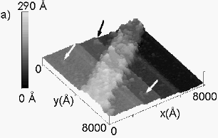
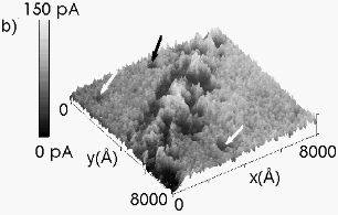
Fig. 14: (a) 3D image of a single quantum wire, (b) corresponding BEEM image. The arrows indicate Au clusters in the etched areas.
Figure 14 (a) shows the topography of a single quantum wire, Fig. 14 (b) the BEEM image, which was measured simultaneously. Two main details are evident: First, there are some Au-clusters accumulated on the wire, which are reflected as dark areas in the BEEM image. This cluster formation depends on sample preparation and was avoided in most recent measurements. Second, the BEEM current is slightly enhanced on the wire. This enhancement becomes clear if one looks at the bandstructure of the etched and non etched areas of the quantum wire sample. As one can see in Fig. 15 (a) the effective surface barrier height is higher in the etched areas, since here, the AlGaAs barrier under the surface is higher than the barrier of the Au-GaAs Schottky contact.. Thus, the corresponding BEEM current is lower than in the non etched areas on the quantum wire. To prove this experimentally, the barrier height was measured across the quantum wire and Fig. 15 (b) shows the experimental data. Detailed investigations on this topic are currently in progress.
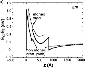
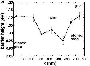
Fig. 15: (a) self consistently calculated bandstructure; (b) measured barrier height profile across a quantum wire.
Studies on the Lifetime of Intersubband Transitions in Semiconductor Superlattices (K. Unterrainer, R. Zobl, G. Strasser)
In unipolar semiconductors laser operation can only be achieved by a population inversion of charge carriers, which is governed by the lifetime of electrons (or holes) in excited states. In this work, the lifetime of electrons in excited states is investigated. In the last year pump and probe experiments on samples designed, grown, processed and tested in the MISZ were performed using the free electron laser "FELIX" in Nieuwegein (the Netherlands). The measured lifetimes of 400 ps in GaAs/AlGaAs are compared to calculated results of a theoretical model. This comparison shows that a combination of electron-electron scattering and optical and acoustical phonon scattering is limiting the electronic lifetime. In the running project asymmetric coupled quantum wells with a more sophisticated bandstructure and therefore a more complex level system are grown to test the possibility of subband inversion. Besides a deeper understanding of lifetimes in coupled wells a long-term goal is the development of an optically pumped FIR-semiconductor laser.
Ballistic Electron Spectroscopy of Biased Vertical Superlattices (C. Rauch, G. Strasser, K. Kempa, K. Unterrainer, W. Boxleitner)
The splitting of minibands in biased superlattices has direct consequences on the ballistic electron transport properties. Due to the localization of the electron wave function, the quasi-continuous miniband breaks up into a ladder of discrete Wannier-Stark states.
Using the concept of a hot electron transistor the transmittance of an undoped superlattice, grown in the drift region between base and collector, can be measured directly.
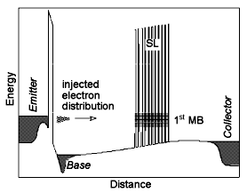
Fig. 16: Conduction band diagram of a three terminal device under typical bias conditions
An energy tunable electron beam is generated by a tunneling barrier and used to probe ballistic transport through the superlattice at given bias conditions (Fig. 16). The collector current is measured as a function of the injection energy. The probability for an injected hot electron to cross the superlattice reflects the transmittance of the discrete ladder of Stark states and can be considered to be proportional to the measured transfer ratio (a = IC/IE).
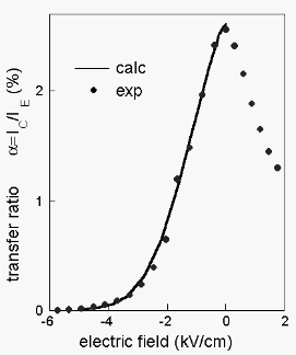
Fig. 17: Measured (dots) and calculated (line) transfer ratio vs. electric field
Figure 17 shows the transfer ratio of a ten period GaAs/AlGaAs superlattice versus electric field. The maximum transmission can be observed at zero bias voltage, since all superlattice states are extended over the whole superlattice dimension. Applying an electric field leads to a decrease of the transmission due to the localization of the lowest and uppermost superlattice states, i.e., these states do not contribute to the ballistic transport any more. The transfer ratio of the superlattice vanishes for an applied electric field of about 5 kV/cm. This is in good agreement with the simple estimate of the localization length l »
D/eF (D is the miniband width, and F the applied electric field) which decreases to about half of the total superlattice length at this bias.
In addition, we perform theoretical calculations based on a transfer matrix method using an envelope function approximation. The solid line in Fig. 17 shows the result of such a calculation for the measured structure. We find an excellent agreement between our experimental results and the quantitative theoretical prediction.
For the first time, the collapse of the superlattice states under electrical field can be observed directly using the technique of ballistic hot electron spectroscopy. To resolve the discrete Wannier Stark states, we designed a Four Terminal Device (FTD) including a resonant tunneling diode as an injector in order to decrease the width of the injected electron distribution.
Electron Transport Through a Combination of Different Superlattices (C. Rauch, G. Strasser, E. Gornik)
In this report we summarize the results obtained by hot electron spectroscopy of combinations of field free undoped superlattices. The study was carried out using a modified tunneling hot electron transfer amplifier, with an injector consisting of a tunneling barrier embedded within two highly doped GaAs contact layers. An energy tunable electron beam is injected into the structure under investigation. The measured static transfer ratio is defined by the ballistic electron current measured at the collector of the three terminal device divided by the emitter current (a = IC/IE). Since the transfer ratio is proportional to the transmittance of the structure, which is grown between the base and the collector contact, we get important information of the transport mechanism in such sophisticated quantum mechanical systems.
The samples grown by Molecular Beam Epitaxy we have studied consist of the following common features: A highly doped n+-GaAs collector contact layer (n = 1x1018 cm-3) is grown on a semiinsulating GaAs substrate. Followed by the heterostructure under investigation and the drift regions which are slightly n-doped (~
5x1014 cm-3), in order to avoid undesired band bending. These layers are followed by a highly doped (2x1018 cm-3) n+-GaAs layer (base) of 13 nm width. On top of the base layer a 13 nm undoped Ga0.7Al0.3As barrier is grown followed by a spacer and an n+-GaAs layer, nominally doped to n = 3x1017 cm-3. Finally, a n+-GaAs contact layer (n = 1x1018 cm-3) is grown on top of the heterostructure to form the emitter. The full width at half maximum (FWHM) of the injected energy distribution was measured to be 17 meV in width using a resonant tunneling diode in the drift region. It should be noted that the FWHM limits the energy resolution.
The fabrication (Fig. 18) of the three terminal device includes the following steps: SiCl4/SF6 reactive ion etching (RIE), unselective etching to the collector layer, metallization of the AuGeNi ohmic contacts, Si3N4 insulation of the emitter mesa (PECVD), and finally the metallization of the CrAu bonding pads.
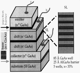
Fig. 18: Three terminal device
We have grown two samples with different combinations of five period superlattices. The superlattice growth parameters are given in the table below.
|
sample No. |
superlattice 1 |
superlattice 2 |
superlattice 3 |
| |
barrier (Å) |
well (Å) |
barrier (Å) |
well (Å) |
barrier (Å) |
well (Å) |
|
1 |
35 |
42.5 |
25 |
120 |
|
|
|
2 |
35 |
42.5 |
25 |
120 |
15 |
85 |
Sample No. 1 consists of two superlattices. The parameters were chosen in such way that the lowest miniband of the first superlattice is aligned with the second miniband of the second superlattice. Injected electrons with energies high enough to traverse into the lower miniband of the first superlattice have two output channels. One channel is defined by transport through the second miniband of the second superlattice without scattering. Electrons which are scattered in the second miniband can be collected via transport through the first miniband of the second superlattice.
Sample No. 2 consists of three different superlattices as noted in the table. The conduction band structure is sketched in Fig. 19. The first and the second superlattice have the same parameters as the superlattices in sample No. 1. The third superlattice is designed such that the minigap between the first and the second miniband is aligned with the second miniband of superlattice 2. The first minibands of superlattice two and three are aligned as well. Consequently only electrons which are scattered in the second superlattice can be collected and measured in the collector current. Electrons that are reflected by the minigap and not scattered into the first miniband will be bounced back and collected at the base layer.
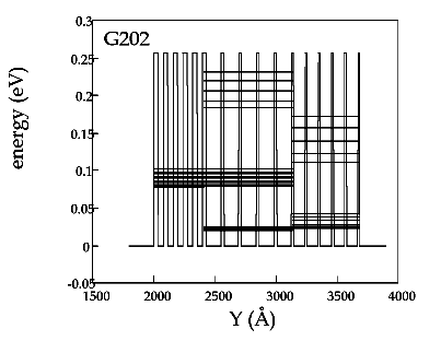
Fig. 19: Bandstructure of a combination of three different superlattices
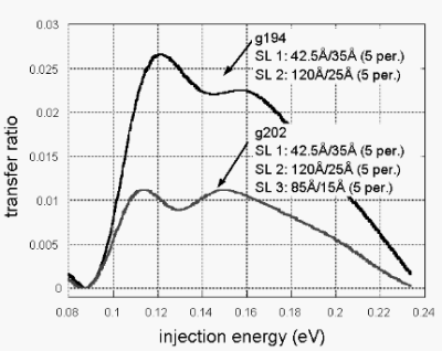
Fig. 20: Comparison of the transfer ratio of two different combinations of superlattices
In Fig. 20 the transfer ratio a versus injection energy is shown. A sharp increase of the transfer ratio is evident at about 90 meV which corresponds to the position of the first miniband of superlattice 1. It can be seen that the transfer ratio of sample No. 2 is about 50 % of the transfer ratio of sample No. 1. Consequently we assume that about half of the electrons injected into the second miniband of the second superlattice are scattered into the first miniband. Since the energy gap between the second and the lowest miniband is of the order of an longitudinal optical (LO) phonon, we know that the interminiband transition is mainly governed by LO-phonon scattering which is the most effective scattering process at low temperatures. If the minigap is smaller than 36 meV one might achieve inversion and consequently a light emitting device. The design of such a structure is even more sophisticated. A prototype of a sample mentioned above is already grown and will be characterized soon.
Coherent Few-Cycle THz Emission from Plasmons in Bulk GaAs (R. Kersting, K. Unterrainer, G. Strasser, E. Gornik)
Femtosecond optical excitation of bulk semiconductors leads to the emission of coherent far infrared pulses. This emission results from instantaneous polarization, ballistic transport and drift of photogenerated carriers in the surface or built in fields of semiconductors. We have investigated the generation of few-cycle THz radiation from coherent plasmons in bulk GaAs.
For the first time our experimental data give direct insight into two distinctly different emission processes: THz generation by plasma oscillations of hot photogenerated carriers, and THz emission from coherent oscillations of cold extrinsic carriers.
The upper curve of Fig. 21 shows the autocorrelation of a THz pulse emitted from a p-i-n structure after femtosecond laser excitation. By increasing the excitation density, coherent emission can be found between 0.2 and 1.5 THz. The frequencies vary as the square root of the excitation density, as expected for plasmons. This proves that the THz emission results from the plasma oscillation of the photogenerated carriers. We find that the emitted THz radiation from the p-i-n diode is strongly damped. We attribute this to the fact that the photogenerated carriers are hot and thus subject to fast scattering processes.
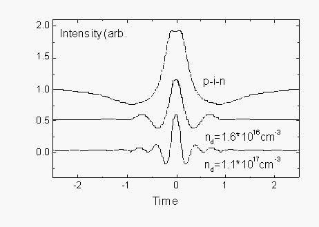
Fig. 21: Autocorrelation data recorded on the p-i-n structure and on two bulk GaAs structures with different doping concentrations.
A fundamentally new emission process is found in n-doped bulk GaAs. Here, the screening of the surface field by photogenerated carriers starts coherent oscillations of the extrinsic carriers in the GaAs bulk. Autocorrelation data are shown by the lower curves in Fig. 21. In contrast to the results on p-i-n structures the frequencies of these THz pulses depend on the doping concentration but not on the density of the photogenerated carriers. This shows that the THz radiation is emitted by the oscillation of the extrinsic electrons in the GaAs bulk. The damping times of these oscillations are much slower than in p-i-n structures which leads to multiple oscillations of the field. We show that the oscillations of the cold carrier plasma are limited to the center of the Brillouin zone and that the damping of the extrinsic plasma oscillations results mainly from optical phonon scattering.
Since the emitted power of the THz radiation strongly depends on the damping rate the cold plasma oscillation in bulk GaAs offer an attractive approach to generate intense THz pulses. Our experiments show that the emission power on n-doped structures is more than one order of magnitude higher than the power emitted from diode structures.
Photonic Bandgap Material Used as THz Resonators (K. Unterrainer, R. Kersting)
For the realization of a THz-laser an efficient coupling structure and resonator is needed. The resonator is defined by two photonic band gap mirrors which have been already developed at the institute (Fig. 22). Photonic band gap materials show high reflectivity in the THz range. Bow Tie antennas, connected via air bridges to the active mesa to avoid parasitic capacities will be used to couple out the emitted light. At the moment these new processes represent the main activities in this project.
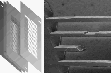
Fig. 22: Photonic band gap material.
Quantum Cascade Electroluminescence in GaAs/AlGaAs Structures (G. Strasser, M. Helm, L. Hvozdara, P. Kruck, E. Gornik)
The advent of a unipolar semiconductor laser based on intersubband transitions in quantum wells [1] in 1994 marked a breakthrough in the application of band-structure engineering. Since then, great progress concerning device operation and performance of these so-called quantum cascade lasers has been achieved [2], however, these results were restricted to a single research laboratory and to a single material system, namely InGaAs/InAlAs lattice matched to InP.
We present here the design, growth and operation of an unipolar light emitting diode (LED) based on the material system GaAs/AlGaAs.
The structure essentially follows the design considerations given by Faist et al. [2], [3] with the modifications necessary due to the different material system. The diode (grown on a semi-insulating GaAs substrate) consists of 25 active periods of GaAs/ Al
0.45Ga0.55As coupled quantum well layers. The growth sequence of the active cell is 10 Å GaAs, 15 Å AlGaAs, 45 Å GaAs, 20 Å AlGaAs, and 45 Å GaAs (see also Fig. 23). The active cells are separated by miniband funnel injectors and the whole structure is embedded between two highly doped contact layers. The LED is designed for emission at about 6.5 µm, but longer or shorter wavelengths than this appear possible. The present choice was dictated by two considerations: on the one hand, shorter wavelength emission (or lasing) is generally easier to achieve due to the larger spontaneous emission rate and smaller losses. On the other hand we wanted to keep the Al content in the barriers below 45% in order to avoid effects related to the X-point.
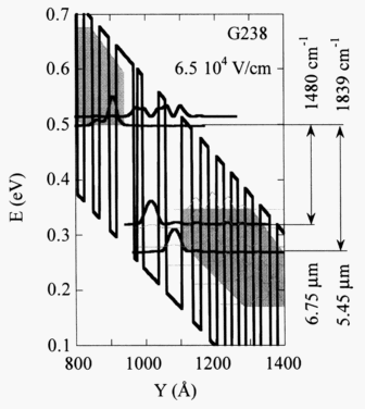
Fig. 23: Self-consistent calculations of the conduction band and the relevant wavefunctions (YY*) under bias
The structure was characterized by measuring the current-voltage characteristics as well as the intersubband absorption and photocurrent under near-zero bias.
Emission measurements were performed with a step-scan Fourier-transform spectrometer using lock-in techniques. 100 x 100 µm2 size mesa structures were employed, which led to a current of the order of 100 mA under injection conditions (bias 8 V). Electrical pulses of typically 15 µs length with a 3 kHz repetition rate were applied to the sample (5% duty cycle). The sample was kept at around 10 K in a LHe flow cryostate and the emission was detected with a LN2 cooled HgCdTe detector.
A typical emission spectrum is shown in Fig. 24. The main emission peak (at 1450 cm-1) is due to the 3-2 transition, but a second peak at higher energy resulting from the 3-1 transition is also visible. Figure 23 shows the calculated band structure under injection bias conditions, the energy-level line-up being in good agreement with the experimental results.
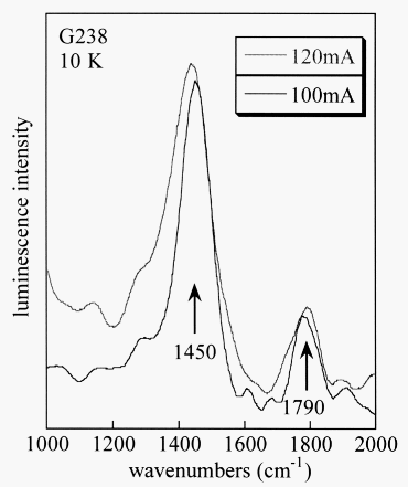
Fig. 24: Electroluminescence at 10 K
First attempts to fabricate a laser structure indicated difficulties with the electrical properties of the AlGaAs waveguide cladding layer. Thus most likely new concepts for optical mode confinement have to be developed in order to achieve a quantum cascade laser based on GaAs.
References
[1] J. Faist, F. Capasso, D. L. Sivco, C. Sirtori, A. L. Hutchinson, and A. Y Cho, Science 264, 553 (1994)
[2] J. Faist, F. Capasso, C. Sirtori, D. L. Sivco, J. N. Baillargeon, A. L. Hutchinson, S.N.G. Chu, and A. Y. Cho, Appl. Phys. Lett. 68, 3680 (1996)
[3] J. Faist, F. Capasso, C. Sirtori, D. L. Sivco, A. L. Hutchinson, S.-N. G. Chu, and A. Y. Cho, Appl. Phys. Lett. 64, 1144 (1994)
Project Information
Project Manager
Univ.-Prof. Dr. Erich Gornik
Institut für Festkörperelektronik, Technische Universität Wien, A-1040 Vienna
Project Group
|
Last Name |
First Name |
Status |
Remarks |
|
Auer |
Peter |
student |
|
|
Eder |
Claudia |
dissertation |
|
|
Finger |
Norman |
dissertation |
|
|
Fürböck |
Christoph |
dissertation |
|
|
Gianordoli |
Stefan |
student |
|
|
Golshani |
Alireza |
dissertation |
|
|
Gornik |
Erich |
Full Prof. |
|
|
Habas |
Predrag |
Post Doc |
|
|
Haider |
Manfred |
student |
|
|
Hainberger |
Rainer |
dissertation |
|
|
Hauser |
Markus |
Post Doc |
50% GMe funding |
|
Hvozdara |
Lubos |
dissertation |
25% GMe |
|
Kellermann |
Peer Oliver |
student |
|
|
Köck |
Anton |
Assistant Prof. |
|
|
Kröll |
Peter |
technician |
|
|
Langmann |
Gottfried |
technician |
|
|
Liu |
Jian |
student |
|
|
Ploner |
Guido |
dissertation |
|
|
Pogany |
Dionyz |
guest scientist |
|
|
Prinzinger |
Johannes |
technician |
|
|
Rauch |
Christoph |
dissertation |
|
|
Roßkopf |
Valentin |
dissertation |
100% GMe |
|
Schrenk |
Werner |
student |
|
|
Seliger |
Norbert |
dissertation |
|
|
Smoliner |
Jürgen |
Assistant Prof. |
|
|
Strasser |
Gottfried |
Assistant Prof. |
|
|
Unterrainer |
Karl |
Assistant Prof. |
|
|
Zobl |
Reinhard |
student |
|
|
Zotl |
Ernst |
student |
|
Publications in Reviewed Journals
A. Golshani, P.O. Kellermann, A. Koeck and E. Gornik and L. Korte, "Surface Emitting Laser Diode Array for Wavelength Division Multiplexing Based on Post Growth Adjustment of Surface Mode Emission", Submitted to Appl. Phys. Lett. Feb. 1997
P.O. Kellermann, A. Golshani, A. Koeck, E. Gornik, H.P.Gaugel, R. Winterhoff, J. Kuhn, "Single-mode and single-beam surface emission from visible red GaInP/AlGaInP laser diodes", to be published in Appl. Phys. Lett. 1997
A. Golshani, A. Koeck, S. Freisleben, C.Gmachl, E. Gornik, L. Korte, "Adjustable surface emission from AlGaAs/GaAs laser diodes based on first-order-grating-coupled surface mode emission", Appl. Phys. Lett. 69 (16), 2312 (1996)
A. Koeck, A. Golshani, R. Hainberger, E. Gornik; L. Korte, "Single-mode and single-beam emission from surface-emitting laser diodes based on surface mode emission", Appl. Phys. Lett, 69 (24), 3638 (1996)
C. Gmachl, A. Golshani, A. Koeck, E. Gornik; J.F. Walker, "Vertical-cavity surface-emitting lasers with monolithically integrated modulators" in Microcavities and Photonic Bandgaps: Physics and Applications; editted by John Rarity and Claud Weisbuch; Nato ASI Series vol. E 324; Kluwer Academic Publishers, Netherlands, p. 387 (1996)
C. Eder, J. Smoliner, "Local barrier heights on quantum wires determined by ballistic electron emission spectroscopy", Appl. Phys. Lett. 68, 2876 (1996)
J. Smoliner, C. Eder, G. Böhm, G. Weimann, "Low temperature current imaging spectroscopy on wet chemically etched quantum wires", Appl. Phys. Lett. 69, 52 (1996)
J. Smoliner, C. Eder, G. Strasser, G. Böhm, G. Weimann, "STM studies on quantum wire structures in air and liquid helium", Superlattices and Microstruct., Vol. 20, 261, (1996) (Proc. NANOMES 96 Symposium, SantaFe)
C. Eder, J. Smoliner, G. Strasser, "BEEM Studies on GaAs-AlGaAs quantum wire structures", Superlattices and Microstruct., Vol. 20, 357, (Proc. NANOMES 96 Symposium, SantaFe)
M. Hauser, J. Smoliner, C. Eder, G. Ploner, G. Strasser, E.Gornik, "Single Quantum Dots as Scanning Tunneling Microscope Tips", to be published in Superlattices and Microstructures (1996) (Proc. NANOMES 96 Symposium, SantaFe)
M. Hauser, J. Smoliner, C. Eder, G. Ploner, G. Strasser, E.Gornik, "Scanning Tunneling Microscopy with Single Quantum Dot Tips", Phantoms Newsletter, 12, 1 (1996)
C. Eder, J. Smoliner, G. Böhm, G. Weimann, "Room temperature current imaging tunneling spectroscopy of GaAs/AlGaAs quantum wires at ambient pressure", Semicond. Sci. Technol., 11, 1239, (1996)
C. Eder, J. Smoliner, G. Strasser and E. Gornik, "Ballistic electron emission microscopy in liquid helium using low dimensional collector electrodes", Appl. Phys. Lett. 69, 1725, (1996)
T.P. Sosin, W. Treciakowski, M. Leszczynski, G. Strasser,"Biaxial Deformation Effects in Quantum Wells", Proc. ICPS23, Berlin (1996)
W. Boxleitner, C. Rauch, G. Strasser, L. Hvozdara, E. Gornik, U. Meirav, V. Umansky, H. Shtrikman, "Electron Dynamics and Band Structure in high Quality GaAs/AlGaAs Superlattices", Proc. ICPS23, Berlin (1996)
W. Heiss, B.N. Murdin, C.J.G.M. Langerak, S.-C. Lee, G. Strasser, C.R. Pidgeon, I. Galbraith, E. Gornik, M. Helm, "The LO-phonon bottleneck in the intersubband cooling in wide quantum wells", Proc. ICPS23, Berlin (1996)
B.N. Murdin, W.Heiss, C.J.G.M. Langerak, S.-C. Lee, I. Galbraith, G. Strasser, E. Gornik, M. Helm, C.R. Pidgeon, "Direct observation of the LO phonon bottleneck in wide GaAs/AlGaAs quantum wells", Phys. Rev. B 55, 5171 (1997)
C. Rauch, G. Strasser, K. Unterrainer, L. Hvozdara, W. Boxleitner, E. Gornik, "Hot electron spectroscopy of undoped GaAs/GaAlAs superlattices", Superlattices and Microstructures, (to be published)
R. Kersting, K. Unterrainer, G. Strasser, E. Gornik, H.F. Kauffmann, "Coherent Few-Cycle THz Emission of cold plasmons", in Proc. Gordon Research Conference on Laser Interactions with Materials (extended abstract, to be published)
C. Rauch, G. Strasser, K. Unterrainer, B. Brill, E. Gornik, "Ballistic electron spectroscopy of vertical superlattice minibands", Appl. Phys. Lett., 70, 649 (1997)
K.D. Maranowski, A.C. Gossard, K. Unterrainer, E. Gornik, "Far infrared emission from prabolically graded quantum wells", Appl. Phys. Lett., 69, 3522 (1996)
R. Kersting, K. Unterrainer, G. Strasser, H.F. Kauffmann, E. Gornik, "Few-cycle THz emission from cold plasma oscillations", Phys. Rev. Lett. (submitted).
N. Seliger, P. Habas and E. Gornik, "A Study of Backside Laserprobe Signals in MOSFETs", Microelectr. Eng., vol. 31, pp. 87 – 94, January 1996.
N. Seliger, P. Habas and E. Gornik, "Time-Domain Characterization of Lattice Heating in Power VDMOSFETs by Means of an Interferometric Laserprobe Technique", Digest to the European Solid State Device Research Conference (ESSDERC ´96), Bologna, Italy, 9 – 11 September 1996, p. 847
N. Seliger, P. Habas, A. Köck, D. Pogany and E. Gornik, "Backside Laserprobing of Transient Heating in Power VDMOSFETs", Digest to the International Seminar on Power Semiconductors (ISPS ´96), Prague, Czech Republic, 11 – 13 September 1996, p. 115
D. Pogany, N. Seliger, T. Lalinsky, J. Kuzmík, P. Habas, P. Hrkút and E. Gornik, "Study of Thermal Effects in GaAs Micromachined Power Sensor Microsystems by an Optical Interferometer Technique", Digest to the International Workshop on Thermal Investigations of ICs and Microstructures (THERMINIC `96), Budapest, Hungary, 25 – 27 September 1996, p. 185
D. Pogany, T. Lalinsky, N. Seliger, J. Kuzmík, P. Habas, P. Hrkút and E. Gornik: "Power Sensor Microsystems Characterization Using a Contactless Optical Laser Method", Digest to the International Conference of Advanced Semiconductor Devices and Microsystems (ASDAM ´96), Smolenice, Slovakia, 20. – 24.October 1996, p. 201
D. Pogany, N. Seliger, T. Lalinsky, J. Kuzmík, P. Habas, P. Hrkút and E. Gornik, "Study of Thermal Effects in GaAs Micromachined Power Sensor Microsystems by an Optical Interferometric Technique", to be published in Microelectronics Journal, 1997
N. Seliger, P. Habas, D. Pogany and E. Gornik, "Time-Resolved Analysis of Self-Heating in Power VDMOSFETs using Backside Laserprobing", submitted to Solid State Electronics, October 1996
E. Burian, D. Pogany, T. Lalinsky, N. Seliger and E. Gornik, "Thermal Simulation and Characterization of GaAs Micromachined Power Sensor Microsystems", submitted to EUROSENSORS XI conference, February 1997
Presentations
C. Eder, J. Smoliner, G. Strasser, "Low temperature BEEM studies on quantum wires fabricated on GaAs-AlGaAs heterostructures", ICPS23, Berlin (1996)
M. Hauser, J. Smoliner, C. Eder, G. Ploner, G. Strasser, E.Gornik, "Single Quantum Dots as Scanning Tunneling Microscope Tips", NANOMES 96 Symposium, SantaFe
C. Eder, J. Smoliner, G. Strasser, "BEEM Studies on GaAs-AlGaAs quantum wire structures", NANOMES 96 Symposium, SantaFe
J. Smoliner, C. Eder, G. Strasser, G. Böhm, G. Weimann, "STM studies on quantum wire structures in air and liquid helium", NANOMES 96 Symposium, SantaFe
T.P. Sosin, W. Treciakowski, M. Leszczynski, G. Strasser, "Biaxial Deformation Effects in Quantum Wells", Proc. ICPS23, Berlin (1996)
C. Eder, J. Smoliner, G. Strasser, and E. Gornik, "Low Temperature Ballistic Electron Emission Microscopy Studies on GaAs/AlGaAs Heterostructures", SXM2 Workshop, Vienna (1996)
A. Köck, C. Gmachl, A. Golshani, S. Freisleben, E. Gornik, "Oberflächenemittierende Laserdioden", Mauterndorfer Laserseminar, 20 – 23 March 1996, Mauterndorf
A. Koeck, A. Golshani, R. Hainberger, N. Finger, C. Gmachl, E. Gornik; L. Korte, "Quasi-single-mode surface-emitting laser diodes based on surface mode emission", SPIE Proc. Vol. 2682 "Laser Diodes and Applications II" of Photonics West, pp.169 – 175, OE/LASE’96, USA, SPIE Optical Engineering Press (1996)
A. Golshani, R. Hainberger, S. Freisleben, A. Koeck, E. Gornik; C. Gmachl; L. Korte, "Efficient surface emitting AlGaAs/GaAs laser diodes based on first-order-grating-coupled surface mode emission", Proceedings of the "European Gallium Arsenide and related III-V compounds application symposium", 3B4; Paris 5 – 7 June, 1996
A. Koeck, N. Finger, C. Gmachl, A. Golshani, R. Hainberger, E. Gornik; L. Korte, "Single-beam and single-mode emission from surface-emitting laser diodes based on surface mode emission", Int. Conf. on Solid State Devices and Materials, Yokohama 26 – 29 August, 1996, SSDM’96 Extended Abstracts pp. 858, (1996)
A. Golshani, A. Koeck, R. Hainberger, E. Gornik; L. Korte, "Single-beam emission from surface emitting laser diodes based on surface mode emission", Proceedings of the "Conference on Lasers and Electro-Optics (CLEO)/Europe", pp. 28; 8 – 13 September 1996, Hamburg, Germany, 1996
A. Koeck, A. Golshani, R. Hainberger, E. Gornik; L. Korte, "Single-beam and single-mode emission from surface emitting laser diodes based on surface mode emission", Proceedings of the "26th European Solid State Device Research Conference"; pp. 541; 9 – 11 September 1996, Bologna, Italy
R. Hainberger, N. Finger, A. Golshani, A. Koeck, E. Gornik; J.F. Walker "A new concept for a direct optical free-space interconnect without lenses", Proceedings of the "26th European Solid State Device Research Conference"; pp. 537; 9 – 11 September 1996, Bologna, Italy
A. Köck, "Oberflächenemittierende monomodige Laserdioden basierend auf dem Konzept der Oberflächenmodenkopplung", Preisträgervortrag, 46. Jahrestagung der Österreichischen Physikalischen Gesellschaft, 23 – 27 September 1996, Linz
A. Köck, A. Golshani, N. Finger, E. Gornik; L. Korte, "Monomodige Einzelstrahlemission von oberflächenemittierenden Laserdioden basierend auf Oberflächenmodenkopplung (poster), Photonik-Symposium der Volkswagen-Stiftung, 7 – 9 October 1996, Schwäbisch Hall-Hessental, Germany
A. Koeck, A. Golshani, R. Hainberger, E. Gornik; L. Korte, "Single-beam and single mode emission from surface emitting laser diodes based on surface mode emission", Proceedings of the "9th Annual Meeting IEEE Lasers and Electro-Optics Society"; Vol. 1, pp. 125, 18 – 21 November 1996, Boston, MA, USA,
A. Koeck, A. Golshani, R. Hainberger, E. Gornik; L. Korte, "Digital beam steering from surface emitting laser diodes based on surface mode emission", SPIE Proc. Vol. 3001 "In-Plane Semiconductor: from Ultraviolet to Mid-infrared" of Photonics West’97, OE/LASE’97, USA, SPIE Optical Engineering Press (1997)
M. Hauser, J. Smoliner, C. Eder, G. Ploner, E. Gornik, "Single quantum dots as scanning tunneling microscope tips", Superlatt.Microstruct. 20, 623 (1996)
G. Ploner,J. Smoliner,G. Strasser,E. Gornik, "Transport characterization of quantum wires by magnetophonon and magnetic depopulation experiments", ICSMM-9 1996, to be published in Superlatt. Microstructures
G. Ploner, J. Smoliner, G. Strasser,E. Gornik, "Magnetophonon analysis of quantum wire systems", Proceedings ICPS-23, World Scientific 1996
G. Ploner, J. Smoliner, G. Strasser, E. Gornik, "Temperature dependent magnetotransport properties for systems of few quantum wires", Physica B 227, 24 (1996)
C. Rauch, G. Strasser, K. Unterrainer, L. Hvozdara, W. Boxleitner, E. Gornik, "Hot electron spectroscopy of undoped GaAs/GaAlAs superlattices", 9th Int. Conf. on Superlattices, Microstructures and Microdevices, 14 – 19 July 1996, Liege, Belgium.
C. Rauch, G. Strasser, M. Heiblum, E. Gornik, "Ballistische Elektronen-Spektroskopie von Minibändern in GaAs/AlGaAs Übergittern", ÖPG Jahrestagung, 23 – 27 September1996, Linz
C. Rauch, G. Strasser, K. Unterrainer, E. Gornik, "Breakdown of the electron wave function in biased superlattices", Workshop on Periodic Structures, 27 – 31 January 1997, Les Houches, France
R. Kersting, K. Unterrainer, G. Strasser, E. Gornik, H.F. Kauffmann, "Coherent Few-Cycle THz Emission of cold plasmons", Gordon Research Conference on Laser Interactions with Materials, 9 – 14 June 1996, Holderness School, Plymouth, N.H., USA
K. Unterrainer, "Observation of Shapiro steps and direct evidence of Bloch oscillations in semiconductor superlattices", 9th Int. Conf. on Superlattices, Microstructures and Microdevices, Liege, Belgium, 14 – 19 July 1996
K. Unterrainer, "Applications of FIR free electron lasers to non-linear spectroscopy", 15th General Conference of the Condensed Matter Division/EPS, Baveno-Stresa, Italy, 22 – 25 April 1996
K. Unterrainer, "Intersubband Dynamics of Asymmetric Coupled Quantum Wells Studied by THz Optical Rectification", 9th International Winterschool on New Developments in Solid State Physics, Mauterndorf, Austria, 19 – 23 February 1996
N. Seliger, "Backside-Laserprober zur Charakterisierung integrierter Halbleiterbauelemente", oral presentation at SIEMENS Munich, Germany, 7 February 1996
P. Habas, "Analyse thermischer Effekte an Leistungs-MOSFETs und SOI-Bauelementen", oral presentation at SIEMENS Munich, Germany, 7 February 1996
E. Gornik, P. Habas, N. Seliger, D. Pogany, and C. Fürböck: "Characterization of Silicon Devices by a Laser Probe Technique", Jahrestagung Österreichische Physikalische Gesellschaft (ÖPG), Linz, Austria, 24 September 1996
Doctor’s Theses
C. Gmachl, "Frequenzverstimmbare oberflächenemittierende Halbleiterlaserdioden mit vertikalem Resonator", TU Wien, 1996
W. Heiss, "Ferninfrarotspektroskopie an unipolaren Halbleitern — Relaxation und Emission", TU Wien, 1996
S. Michaelis, "Nichtlineare Spektroskopie an GaAlAs-Vielschichtstrukturen zur Bestimmung der optischen Eigenschaften im Bereich der Bandkante", TU Wien, 1996
V. Roßkopf, "Spektroskopie strukturierter Elektronengase", TU Wien, 1996
W. Boxleitner, "Untersuchungen der Smith-Purcell Emission in modulierten Halbleiterstrukturen", in progress
C. Eder, "Raster-Tunnelspektroskopie an Halbleiterstrukturen im Nanometerbereich", in progress
N. Finger, "Herstellung von monomodigen oberflächenemittierenden Laserdioden im 1.5-Mikrometer Bereich", in progress
Ch. Fürböck, "Laserinterferometrie an Leistungsbauelementen", in progress
A. Golshani, "Herstellung von durchstimmbaren oberflächenemittierenden Halbleiterlasern", in progress
R. Heer, "STM-Untersuchungen an Nanostrukturen", in progress
Th. Maier, "Integration von VCSELs und Photodetektoren", in progress
G. Ploner, "Temperaturabhängige Transport- und Tunnelspektroskopie an niedrigdimensionalen Elektronensystemen", in progress
Ch. Rauch, "Emission von Halbleiterstrukturen", in progress
N. Seliger, "Untersuchungen der Ladungsträgerdichte- und Wärmeverteilung in integrierten Halbleiterbauelementen mittels Laserinterferometrie", in progress
S. Senkader, "Physikalische Modellierung und Simulation der Sauerstoffpräzipitation in CZ-Silizium", in progress
Habilitations
K. Unterrainer, "Development of FIR (THz) radiation sources", TU Wien, 1996
J. Smoliner, "Current Transport in Nanostructures", TU Wien, 1996
Cooperations
Siemens AG, Dr. Bernd Borchert and Dr. Lutz Korte, Prof. E. Wolfgang, Dr. M. Stoisiek, Dr. G. Deboy, Dr. G. Sölkner; Dr. S. Görlich, Germany
Institut für Angewandte Chemie Berlin Adlershof e.V., Dr. K. Pfeiffer, Germany
Universität Stuttgart, 4. Physikalisches Institut, Prof. Dr. M.H. Pilkuhn, Germany
TU-München, Walter Schottky Institut, Prof. Weimann, Germany
TU München, Lehrstuhl für Techn. Elektrophysik, Prof. G. Wachutka, Germany
Universität Bremen, Inst. für Festkörperphysik, Prof. Dr. D. Hommel, Germany
RWTH Aachen, Inst. f. Halbleiterelektronik, Prof. H. Kurz, Germany
Centre National de la Recherche Scientific, Laboratoire de Microstructures edt de Microelectronique, B.Etienne, Cedex, France
Interuniversity Microelectronics Center (IMEC), Leuven, Belgium
University of Surrey, Physics Department, Dr. B.N.Murdin, UK
Herriot Watt University, Edinburgh, Prof. C. Pidgeon, UK
Ioffe Physico-Technical Institute, St. Petersburg, Prof. A.A. Andronov, Russia
Norwegian University of Science and Technology, Prof. K. Fossheim, Norwegen
Sub-Micron Center, Weizmann Institute, Rehovot, Prof. M. Heiblum, Israel
Academy of Sciences, High Pressure Research Center, Prof. Treciakowski Prof. Suski, Poland
Academy of Sciences, Institut of Physics, Dr. Bartos, Slowakia
Technische Universität Bratislava, Mikroelektronik, Prof. Csabay, Slowakia
Univ. of California, Lawrence Berkeley Laboratories, Prof. E.E. Haller, USA
University of California, Free-Electron-Laser, Santa Barbara, Prof. J. Allen, USA
Boston College, Dep. of Physics, Boston, Massachusetts, Prof. K. Kempa, USA
EPI MBE Components, St. Paul, Minnesota, USA
Universität Linz, Institut für Halbleiterphysik, Prof. G. Bauer, Doz. Dr. M. Helm
Universität Graz, Institut für Experimentalphysik, Prof. F. Aussenegg
Universität Innsbruck, Institut für Experimentalphysik, Doz. Dr. W. Seidenbusch
Siemens AG Villach, Dr. Prybil
Plansee AG, Reutte, Dr. Willhartitz
Universität Wien, Institut für Physikalische Chemie, Prof. Kauffmann
Universität Wien, Institut für Festkörperphysik, Doz. Dr. R. Höpfel
Universität Leoben, Institut für Physik, Prof. Kuchar
TU Wien, Institut für Angewandte u. Technische Physik, Prof. Ebel, Doz. Schattschneider, Doz. Pongratz
TU Wien, Atominstitut der österreichischen Universitäten,. Prof. Weber
TU Wien, Institut für Analytische Chemie, Prof. Robert Kellner