Single Quantum Dots as Scanning Tunneling Microscope Tips
M. Hauser, J. Smoliner, C. Eder, G. Ploner, G. Strasser, E. Gornik
Institute of Solid State Electronics &
Center of Microstructure Research (MISZ)
TU Wien, A-1040 Vienna, Austria
We report the use of single quantum dot structures as tips on a scanning tunneling microscope (STM). A single quantum dot structure with a diameter of less than 200 nm and a height of 2 µm was fabricated by reactive ion etching. This dot was placed on a 40 µm high mesa and mounted on the tip of a STM. The topography of large structures such as quantum wires or gold test substrates is clearly resolved with such a tip. To check the transport properties of the tip, quantum dot arrays were fabricated on resonant tunneling double barrier structures using the same process parameters. Conventional tunneling spectroscopy clearly resolved the 0D states in our samples. Using a metal substrate as second electrode such STM tips can be used to perform high resolution energy spectroscopy on single dots and free standing wire structures.
Recent advances in micro fabrication technology such as lithography, etching and epitaxial regrowth enabled a reduction of the dimensions of semiconductor devices in a way that tunneling processes in low dimensional systems (1D, 0D) can be studied. First experiments on 1D-1D and 1D-0D tunneling processes were carried out in ultra small, pillar shaped double barrier resonant tunneling diodes (DBRTDs) by Reed et al [1]. On such samples, the resonance structures in the tunneling current were assigned to resonant tunneling processes between 1D states in the emitter region and 0D states inside the quantum well defined by the two barriers [2]. In similar experiments, based on asymmetric DBRTDs, charging effects were also observed [3], [4]. Using a shallow etching process in combination with a side-gate, it was possible to adjust the 0D confinement by varying the gate voltage. The observed resonance structures in the tunneling current were assigned to Coulomb blockade effects [5], [6] as well as to ionized donor atoms [7]. Focused ion beam implantation can also be used to define structures containing quantum dots [8] . Using triple barrier RTDs as starting structure, tunneling processes in coupled quantum dot structures have also been investigated experimentally [9] and theoretically [10] – [12]. The fine structure of the current-voltage characteristic [13] in the above experiments can be explained by strong coupling between 1D subbands in the contact region and 0D states inside the quantum dots.
As main problem for all above sample structures, the formation of contacts to the quantum dots is difficult and requires planarization techniques and recess etching. Using the metal tip of a scanning tunneling microscope [14] as a mobile contact to single wires or quantum dots, however, this problem is overcome and even local tunneling spectroscopy on single wires can be performed [15], [16].
In this paper we report an inverse approach to the above experiments and replace the metal tip of the STM by a single quantum dot on a high mesa. To test the resolution of such a tip, the topography of a gold substrate and also of a large quantum wire array was scanned. To check the electrical quality of the tip, conventional tunneling spectroscopy on double barrier resonant tunneling diodes was employed. The 0D states are clearly resolved in our samples demonstrating that such STM tips are an easy way to establish contacts to single dots and free standing wire structures.
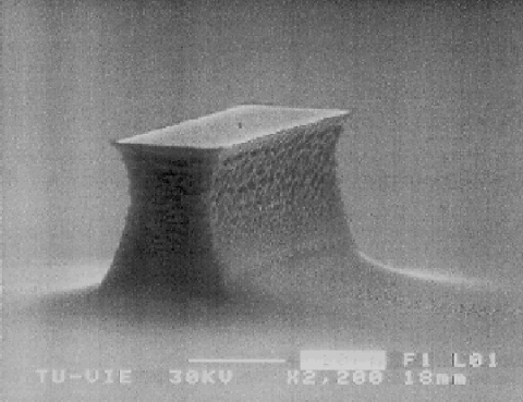
To fabricate the tips, electron beam lithography on a double layer of PMMA / PMMA-MA copolymer resist, metallization and lift off were used to define a single gold dot on a GaAs substrate. Optical lithography and RIE (Ar, SiCl4 and SF6) was then used to define the mesa supporting the dot. Residual photoresist is also removed by this step. The mesa is then etched further by RIE (Ar, SiCl4) processes using the small gold dot as etch mask to produce a thin pillar with 200 nm diameter and 2 µm height (Fig. 1).
Fig. 1: The supporting mesa was defined by optical lithography and RIE. On top of it a single gold dot can be seen defined by electron beam lithography, metallization and lift off. The dot mask is etched into the mesa by further RIE processing to form a single quantum dot. This structure is then used to replace the metal tip of an STM.
This structure was mounted on the STM and used as a superfine STM tip to scan an array of wet chemically etched quantum wires. The result of this experiment is shown in Fig. 2.
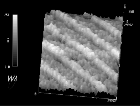
Fig. 2: Wet chemically etched quantum wires scanned with a STM. An etched quantum dot on a high supporting mesa was used as the tip of the STM.
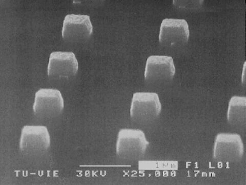
Fig. 3: Top contacts of quantum dots after planarization and recess etching by RIE. The metallized top contacts were used as an etch mask and form together with a second metallization a common top electrode for standard tunneling spectroscopy measurements.
To demonstrate that 0D levels are formed in the etched quantum dot we applied the same fabrication technology to standard RTD structures. An array of quantum dots planarized with resist, recess etched and metallized to form a top contact is shown in Fig. 3. A bias voltage was applied to the quantum dots and the current through the dots was measured in liquid Helium by standard tunneling spectroscopy. Fig. 4 shows the obtained results. Resonant tunneling between 0D states and energy levels in the double barrier can clearly be seen in the current / voltage characteristic around -0.15 V, -0.35 V and -0.7 V. The resonances around -0.15 V are much better resolved in the derivative of the I/V characteristic.
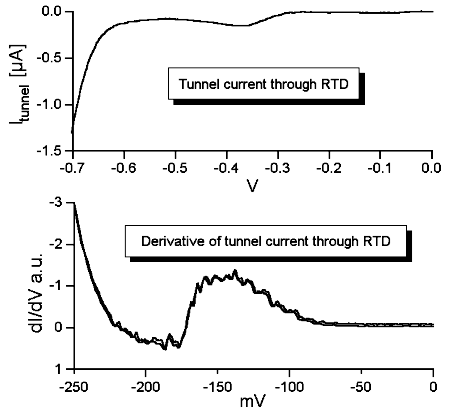
Fig. 4: Top image: IV characteristic of a RTD quantum dot array. Resonant tunneling through energy levels in the double barrier can be clearly resolved at bias voltages of 0.35 V and 0.7 V. Bottom image: Resonant tunneling through 0D energy levels can clearly be resolved in the derivative of the I/V characteristic around a bias voltage of 0.15 V. Similar resonances are also found at 0.35 V and -0.7 V.
Conclusion
In summary, we have used a single quantum dot structure as the tip of a STM. It was found that quantum dot structures with a diameter of less than 200 nm and a height of 2 µm form a very fine tip also suitable of scanning topographic profiles of other nanostructures such as quantum wires. Tunneling processes between low dimensional states on reference samples were also investigated in this configuration. For this purpose, quantum dot arrays were fabricated on resonant tunneling double barrier structures using the same process parameters than for the STM tips. In the RTD dot arrays, 0D states are clearly resolved by conventional tunneling spectroscopy. Thus, our method provides a simple way to for tunneling spectroscopy on single quantum dots, provided the STM is operated at low temperatures. As our STM can be operated in liquid helium [16], further experiments are in progress.
Acknowledgments
This work was also sponsored by Bundesministerium für Wissenschaft, Verkehr und Kunst and Jubiläumsfonds der Österreichischen Nationalbank).
References
[1] M.A. Reed, J.N. Randall, R.J. Aggarwal, R.J. Matyi, T.M. Moore, A.E. Wetsel, Phys. Rev. Lett. 60, 535 (1988).
[2] M. Boero, J.C.Inkson, Phys. Rev.B 50, 2479, (1994)
[3] Bu Su, V.J. Goldman, J.E. Cunningham, Science 255, 313 (1992)
[4] M.Tewordt, L. Martin-Moreno, J.T. Nichols, M. Pepper, M.J. Kelly, V.J. Law, D.A. Ritchie, J.E.F. Frost, G.C.A.Jones Rev. B 45, 14407, (1992)
[5] M. Tedwordt, L. Martin-Moreno, J.T. Nicholls, M. Pepper, M.J. Kelly, V.J. Law, D.A. Ritchie, J.E.F. Frost, G..A.C. Jones, Phys. Rev. B 45, 14407 (1992)
[6] P. Guéret, N. Blanc, R. Germann, H. Rothuizen, Phys. Rev. Lett. 68, 1896 (1992)
[7] M.W. Dellow, P.H. Beton, C.J.G.M. Langerak, T.J. Foster, P.C. Main, L. Eaves, M. Henini, S.P. Beaumont and C.W.D. Wilkinson, Phys. Rev. Lett. 68, 1754 (1992).
[8] S. Tarucha, J. Tokuta, Y. Hirayama, Rev. B 43, 9373, (1991)
[9] M. Tewordt, H. Asahi, V.J. Law, R.T. Syme, M.J. Kelly, D.A.Ritchie, A. Churchill, J.E.F. Frost, R.H. Huges, G.C.A. Josnes, Appl. Phys. Lett., 50, 413, (1987)
[10] C.Y. Fong, J.S. Nelson, L.A. Hemstreet, R.F. Gallup, L.L. Chang, L. Esaki, Phys. Rev. B 46, 9538 (1992)
[11] Zhen Li Ji, Phys. Rev.B 50, 4658 (1994)
[12] M. Tedword, R.J.F. Huges, L.M. Moreno, J.T. Nicholls, H. Asahi, M.J. Kelly, V.J. Law, D.A. Ritchie, J.E.F. Frost, G.A.C. Jones, M. Pepper, Phys. Rev. B 49, 8071, (1994)
[13] G.W. Bryant, Phys. Rev. B 44, 12838, (1991)
[14] G. Binnig, G. Rohrer, Ch. Gerber, E. Weibel, Phys. Rev. Lett. 49, 57 (1982)
[15] C. Eder, J. Smoliner, Appl. Phys. Lett. 68, 2876 (1996)
[16] J. Smoliner, C. Eder, G. Böhm, G. Weimann, Appl. Phys. Lett. 69, 52 (1996)
Project Information
Project Manager
Dr. Jürgen Smoliner
Institut für Festkörperelektronik, Technische Universität Wien, A-1040 Vienna
Project Group
|
Last Name |
First Name |
Status |
Remarks |
|
Eder |
Claudia |
dissertation |
|
|
Hauser |
Markus |
postdoc |
|
|
Heer |
Rudolf |
dissertation |
|
|
Prinzinger |
Johannes |
technician |
|
|
Smoliner |
Jürgen |
assistant professor |
Publications in Reviewed Journals
Presentations
Doctor’s Theses
Habilitations
Cooperations