Ballistic Electron Spectroscopy of Semiconductor Heterostructures
C. Rauch, G. Strasser, K. Unterrainer, E. Gornik
Institut für Festkörperelektronik, TU Wien
A-1040 Vienna, Austria
We present a study of ballistic electron transport in GaAs/GaAlAs with different well widths under given bias conditions. A three terminal device is used to inject an energy tunable electron beam via a tunneling barrier into an undoped superlattice and to collect the transmitted current as a function of the injection energy. Significant increase of the collector current is observed due to miniband conduction in the superlattice. Due to the localization of the electron wave function in biased superlattices, the quasi-continuous miniband breaks up into a ladder of discrete Wannier Stark states. The results are compared to calculations based on an envelope function approximation using a transfer matrix method. In order to resolve the discrete Wannier Stark states, a Four Terminal Device (FTD) is designed.
Introduction
Decreasing the barrier thickness of multiple quantum well structures leads to a stronger coupling between the degenerate eigenstates in the wells and thus to the formation of superlattice (SL) minibands. For these strongly coupled quantum wells the electronic states are extended. Applying an electric field in the direction perpendicular to the layer planes leads to a reduction of the interwell coupling and localizes the electronic states into a finite number of periods. This splitting of the quasi-continuous miniband into a ladder of discrete Wannier Stark states has direct consequences on the ballistic electron transport properties.
A hot electron transistor [1] is used to probe the superlattice transmittance. In such three terminal devices, an energy tunable electron beam is generated by a tunneling barrier, passes the superlattice after traversing a thin highly doped GaAs (base) and an undoped drift region. Having the possibility to drive the injected current and the electric field applied to the superlattice independently, the transmittance can be measured directly at given superlattice biases. The probability for an injected hot electron to cross the superlattice reflects the transmittance of the miniband and can be considered to be proportional to the measured transfer ratio a = IC/IE.
Device Fabrication
Our samples, grown by molecular beam epitaxy (MBE), have the following common features: A highly doped n+-GaAs collector contact layer (n = 1x1018 cm-3) is grown on a semiinsulating GaAs substrate. Followed by a superlattice and the drift regions which are slightly n-doped (~ 5x1014 cm-3), in order to avoid undesired band bending. To reduce quantum mechanical confining effects originating from the quantum well formed by the emitter barrier and the superlattice the drift region is chosen to be at least 200 nm in width. This is followed by a highly doped (2x1018 cm-3) n+-GaAs layer (base) of 13 nm width. As found in previous experiments [2], about 75% of the injected electrons traverse the base ballistically. On top of the base layer a 13 nm undoped Ga0.7Al0.3As barrier is grown followed by a spacer and an n+-GaAs layer, nominally doped to n = 3x1017 cm-3, in order to achieve an estimated normal energy distribution of injected electrons of about 15 meV [3]. It should be noted that the half width of the injected electron beam limits the energy resolution of the experiment. Finally, an n+-GaAs contact layer (n = 1x1018 cm-3) is grown on top of the heterostructure to form the emitter. Four different superlattices have been studied with Ga0.7Al0.3As barriers (2.5 nm) and GaAs wells, with varying widths (6.5 nm, 8.5 nm, and 15 nm) and periods (see table 1).
|
sample # |
well (nm) |
periods |
D 01(meV) |
D MB1(meV) |
D 12(meV) |
D MB2(meV) |
|
1 |
6.5 |
5 |
46 |
22 |
114 |
94 |
|
2 |
8.5 |
5 |
33 |
13 |
85 |
53 |
|
3 |
15 |
5 |
14.5 |
3.5 |
40 |
14 |
|
4 |
6.5 |
10 |
46 |
22 |
114 |
94 |
Table 1: Summary of the superlattice tunneling structures investigated. D MB1 and D MB2 denote the widths of the first and of the second miniband, D 01 the energy position of the first miniband with respect to the conduction band edge and D 12 denotes the width of the minigap between the first and the second miniband.
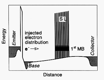
Fig. 1: Conduction band diagram under typical bias conditions.
The fabrication of the three terminal device includes the following steps: SiCl4/SF6 reactive ion etching (RIE), unselective etching to the collector layer, metallization of the AuGeNi ohmic contacts, Si3N4 isolation of the emitter mesa (PECVD), and finally the metallization of the CrAu bonding pads. More details can be found elsewhere [4].
The spatial profile of the bottom of the conduction band along the growth direction under typical bias conditions, as calculated by a Poisson solver, is shown in Fig. 1. All measurements are done in common base configuration at 4.2 K.
Results and Discussion
Unbiased Superlattices
Under flat band conditions the eigenstates of the periodic structure are expected to be extended over the entire length of the superlattice. Using the concept of a hot electron transistor the transmittance of an undoped field free superlattice, grown in the drift region between base and collector, is measured directly. To investigate the superlattice properties and to confirm the results of the measured transfer ratio a = IC/IE, three superlattice structures with different well widths are measured.
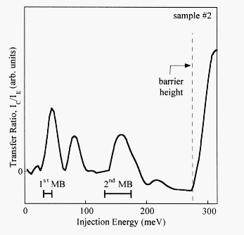
Fig. 2: The transfer ratio a = IC/IE versus injection energy (» e.UEB) of sample #2. The calculated miniband positions are indicated by bars (├───┤).
The static transfer ratio of sample 2, a = IC/IE, plotted in Fig. 2 as a function of the injection energy, shows several maxima and a sharp rise at 280 meV. No current is observed below the energy of the first peak. The position of the first peak coincides very well with the first miniband. Thus, we claim that the first peak is due to miniband transport through the lowest miniband. For energies higher than the first miniband the transfer ratio drops quite significantly since there is no transport possible through the forbidden minigap of the SL. The second observed peak is shifted 36 meV to higher injection energies and is ascribed to the first LO-phonon emission replica (h w LO = 36 meV) of the injected electron distribution. The relative position in energy and width are equal to that of the first peak. The energy range of electrons injected at voltages corresponding to this second peak is in the forbidden band and no contribution is expected from electrons which have not lost energy due to optical phonon emission. The peak at 150 meV represents transport through the second SL miniband. For an analysis of the observed features we compare the experimental data with the theoretically calculated miniband positions. The calculated positions and widths of the first and second miniband are indicated by bars. The sharp rise of the transfer ratio at 280 meV is due to the transition to continuum. This energy, which corresponds to the conduction band offset of the superlattice barriers, gives us a confirmation of the AlAs mole fraction of the AlGaAs compound.
In Fig. 3 we show the transfer ratio a as a function of the injection energy for three samples with different well widths at lower injection energies. There is a clear shift of the peaks to higher energies with decreasing superlattice well width. The calculated miniband positions are again indicated by bars as in Fig. 2. It can be seen that the tunneling data agree very well with the self constant solution of the Schroedinger equation. Note that it is possible to resolve even very narrow minibands at low energies as seen for sample 3.
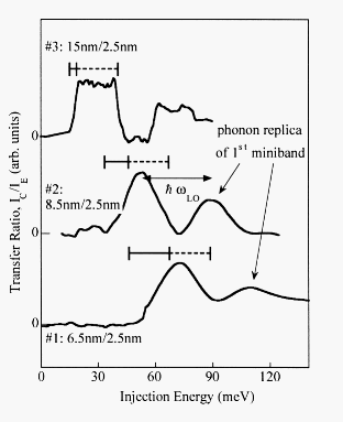
Fig. 3: Transfer ratio a versus injection energy for all three samples ( ├──┤ indicates the calculated miniband position, ├ ─ ┤ indicates the broadening due to the energy distribution of the injected electron beam). A double arrow represents the energy of a longitudinal optical phonon (h w LO = 36 meV).
Due to the broadened energy distribution of the injected electrons, the peaks corresponding to ballistic transfer through the first miniband are broadened as well. The shape of the energy distribution is investigated using a three terminal device with a resonant tunneling diode grown in the drift region which acts as an energy filter of the injected electrons [5], [6]. Thus we are able to measure directly the injected normal energy distribution. It can be seen that this energy distribution is not symmetric and the broadening takes place mainly at the low energy side. This low energy tail of the injected electron beam is indicated by dashed bars in Fig. 3.
Biased Superlattices — Breakdown of the Extended Electron Wave Function
The splitting of minibands in biased superlattices has direct consequences on the ballistic electron transport properties. Due to the localization of the electron wave function, the quasi-continuous miniband breaks up into a ladder of discrete Wannier-Stark states [7].
The transfer ratio of a biased 10 period superlattice (sample 4) was studied and compared with a theoretical transfer matrix calculation. The structure under investigation is except the number of periods similar to the structure described above.
The measured transfer ratio a as a function of the normal electron injection energy at different collector-base biases is shown in Fig. 4. It can be seen that the onset of the transfer ratio shifts with the applied collector-base bias since the lower edge of the first miniband shifts with the superlattice bias. The observed transfer ratio decreases quit dramatically with the applied electric field. Longitudinal optical phonon replicas, which are shifted 36 meV to higher injection energies, can be observed at all biases.
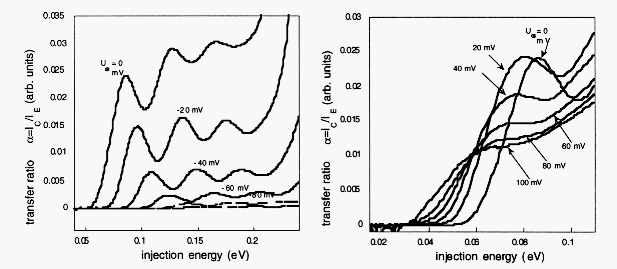
Fig. 4: Measured transfer ratios at different collector-base bias vs. injection energies
Figure 5 shows the transfer ratio at peak position of the investigated superlattice versus applied electric field. The maximum transmission can be observed at zero bias voltage, since all superlattice states are extended over the total superlattice dimension. Applying an electric field leads to a decrease of the transmission due to the localization of the lowest and uppermost superlattice states i.e. these states do not contribute to the ballistic transport any more. The transfer ratio of the superlattice vanishes for an applied electric field of about 5 kV/cm. This is in good agreement with the simple estimate of the localization length l » D/eF (D is the miniband width, and F the applied electric field) which decreases to about half of the total superlattice length at this bias.
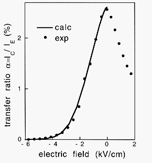
Fig. 5: Measured (dots) and calculated (line) transfer ratio vs. electric field.
In addition, we perform theoretical calculations based on a transfer matrix method using an envelope function approximation [8]. The solid line in Fig. 5 shows the result of such calculation for the measured structure. We find an excellent agreement between our experimental results and the quantitative theoretical prediction.
For the first time, the miniband positions, widths, and the collapse of the superlattice states under the influence of an applied electrical field using the technique of hot electron spectroscopy is observed directly.
Four Terminal Device (FTD)-Detection of Plasmon Emission
A new four terminal device is developed including a resonant tunneling diode as an injector in order to decrease the width of the injected electron distribution. As the resonant condition of the injector resonant tunneling diode is set, we are able to tune the injected sharp electron beam. This device is used to observe directly the relaxation of hot carriers via plasmon emission in a low doped (n = 3x1017 cm-3) GaAs drift region which is contacted to the ground in order to avoid undesired charging in this drift region.
In between this low doped drift region and the collector an analyzer resonant tunneling diode is grown. A SEM picture of the device is shown in Fig. 6. A schematic sketch of the band diagram is shown in the inset of the figure. The four terminal device is also being considered as a structure which allows the possibility to set up conditions for the beam plasma instability leading to local oscillations of charge densities and consequently to an emission of radiation in the THz range.
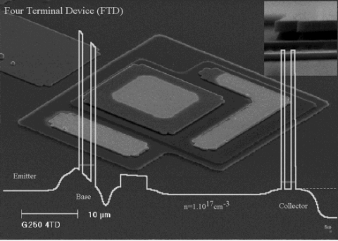
Fig. 6: SEM picture of the Four Terminal Device (FTD). The inset shows the conduction band structure.
In addition the four terminal device design is used to resolve the single Stark states of a short period superlattice, since the injected electron distribution is much narrower than the spacing between the single states.
Conclusion
In summary, direct experimental current spectroscopy of minibands in undoped superlattices is demonstrated using the technique of hot electron spectroscopy. Miniband widths and gaps of different unbiased superlattices are investigated and compared to the results of a self-consistent Schroedinger calculation. Applying an electric field to the superlattice the quasi-continuous miniband splits up into a discrete ladder of Stark states, and consequently the transmission of ballistic electrons decreases. The measured transfer ratio at different bias conditions is in excellent agreement to the theoretical calculation based on a transfer matrix method using an envelope function approximation. For the first time, the collapse of the superlattice electron states under the influence of an electrical field is observed directly in transport.
In order to increase the resolution of the experiment and in order to measure the relaxation of hot carriers via plasmon emission, a four terminal device (FTD) is designed and fabricated.
Acknowledgment
We are very grateful to K. Kempa for his calculations of the transmission of superlattices and for many helpful discussions. This work was partly supported by the Austrian Federal Ministry of Science, the Society for Microelectronics (GMe, Austria), and the European Research Office (project N68171-96).
References
[1] M. Heiblum, M.I. Nathan, D.C. Thomas, and C.M. Knoedler, Phys.Rev.Lett. 55, 2200 (1985)
[2] B. Brill, to be published (1997).
[3] S. Bending, A. Peck, J. Leo, K.v. Klitzing, P. Gueret, and H.P. Meier, Solid-State Electronics 32, 1161 (1989).
[4] C. Rauch, G. Strasser, K. Unterrainer, and E. Gornik, Appl. Phys. Lett. 70, 649 (1997); B. Brill and M. Heiblum, Phys. Rev. B 49, 14762 (1994)
[5] G. Strasser, C. Rauch, and E. Gornik, "Normal energy distribution of a tunneling injector", to be published
[6] M. Heiblum and M.V. Fischetti, IBM J. Res. Develop. 34, 530 (1990).
[7] G.H. Wannier, Elements of Solid State Theory (Cambridge University Press, London, 1959), pp. 190-193.; L. Esaki, and R. Tsu, IBM J. Res. Dev. 14, 61 (1970).
[8] G. Bastard, Phys. Rev. B 24, 5693 (1983).
Project Information
Project Manager
Dr. Gottfried Strasser
Institut für Festkörperelektronik, Technische Universität Wien, A-1040 Vienna
Project Group
|
Last Name |
First Name |
Status |
Remarks |
|
Hvozdara |
Lubos |
dissertation |
25% GMe funding |
|
Kröll |
Peter |
technician |
|
|
Rauch |
Christoph |
dissertation |
|
|
Strasser |
Gottfried |
assistant professor |
Publications in Reviewed Journals
Presentations
Doctor’s Theses
Cooperations