Electron-Beam Lithography for Novel Devices
E. Zotl, M. Hauser, G. Strasser, E. Gornik
Institute of Solid State Electronics &
Center of Microstructure Research (MISZ), Techn. Univ. Vienna
A-1040 Vienna, Austria
The goal of this project was the production of a planar Schottky diode with integrated bow-tie antennas. Due to the planar structure of this device it can be easily implemented into integrated circuits, making it attractive for use as a Terahertz detector. Because of the importance of the RC product for high frequency applications one has to minimize the size of the Schottky contact. This can be achieved by electron-beam lithography and a new combination of positive and negative lithography processes, which allows the production of contacts with typical diameters of 100 nm. Furthermore, a first electrical characterization was made.
Introduction
Metal-semiconductor junctions are known since the end of the last century [1]. Point-contact diodes have been used for detector- and mixer-applications in the millimeter region for decades. Their parameters strongly depend on the manufacturing process, which causes poor reproducibility.
With the development of new technologies like MBE (molecular beam epitaxy) or evaporation of metals it was possible to increase the quality of the Schottky contacts. Although point-contact diodes are used in various applications, it is desirable to develop planar Schottky-diodes with integrated receiving antennas which can easily be implemented into existing electronics.
If one wants to extend the range of operation of the Schottky diode into the THz range, some problems have to be considered:
The parasitic capacitance can be reduced by integrating the contact pads into the antennas. By use of electron beam lithography defined airbridges it is possible to reduce the contact areas to dimensions of 100 x 100 nm.
Submicron Schottky Diodes
Fabrication
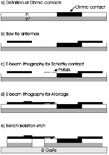
A new processing technology for the fabrication of planar terahertz diodes has been developed utilizing electron-beam lithography and trench isolation. The major processing steps are summarized in Fig. 1.
Fig. 1: Fabrication process of the submicron Schottky diode.
The first step was the evaporation of Ni/Ge/Au ohmic metal on the surface of the etched n+-layer surrounding the active area. The bow tie antennas were defined by conventional photolithography. In the next step, a narrow line (200 nm) was defined in the active region of the diode by electron beam lithography (EBL) in a positive process. After that it was necessary to irradiate the region surrounding the narrow line with an electron dose high enough to crosslink the macromolecules of the resist. This is needed for the isolation between the airbridge and the n-layer. Definition of the airbridge by EBL and evaporation of gold followed. The bow tie antennas were finally isolated by a deep trench etching down to the semi-insulating substrate. Scanning electron microscope pictures of the fabricated device and the Schottky contact are shown in Fig. 2 and Fig. 3.
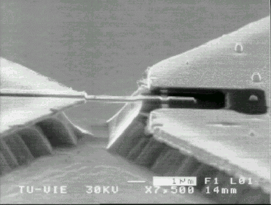
Fig. 2: SEM picture of the device including the airbridge and the Schottky contact.
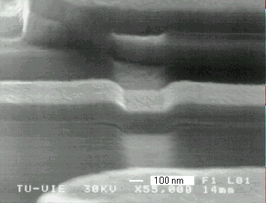
Fig. 3: SEM picture of the Schottky contact.
Measurements
The measurement of the I-V-curve (see Fig. 4) of the Schottky diode allowed the extraction of important parameters regarding the estimation of the working frequency of this device. The series resistance of the diode was found to be 150 Ohm.
The capacity of the Schottky contact can be calculated from the contact area and the width of the depletion region [2]. From a contact area of 200 nm x 250 nm follows a capacity of 1 fF, which results in a cut-off frequency of 11 THz.
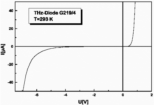
Fig. 4: I-V-curve of the Schottky diode.
Conclusion
A planar Schottky diode with integrated bow-tie antennas was fabricated. The process which was used for this device does not use ion implantation but etching techniques, simplifying the fabrication process drastically. First DC-measurements showed that it is possible to use this Schottky diode as a terahertz-detector. Measurements in the far infrared have to be done in the near future.
[1] F. Braun: "Über die Stromleitung durch Schwefelmetalle", Ann. Phys. Chem., 153, 1874, pp. 556.
[2] J.T. Louhi: "Dynamic Shape of the Depletion Layer of a Submillimeter-Wave Schottky Varactor", IEEE Trans. Microwave Theory Tech., 44, 1996, pp 2159
Project Information
Project Manager
Dr. Markus Hauser
Institut für Festkörperelektronik, Technische Universität Wien
Project Group
|
Last Name |
First Name |
Status |
Remarks |
|
Kersting |
Roland |
postdoc |
|
|
Prinzinger |
Johannes |
technician |
|
|
Strasser |
Gottfried |
assistant professor |
|
|
Zotl |
Ernst |
student |
Publications in Reviewed Journals
Presentations