High Precision Depth Profiles with SIMS
H. Hutter, K. Piplits, M. Gritsch
Institute of Analytical Chemistry, Vienna University of Technology
A-1060 Vienna, Austria
This contribution demonstrates applications of surface analysis techniques for the investigation and characterization of materials and production processes. SIMS depth profile measurements of erbium in silicon demonstrate that high precision measurements of low concentrations are necessary to assist implantation and simulation groups. Measurements of the internal structure of light-emitting diodes verify that the development of new microelectronic components is a great challenge for analytical chemistry.
Introduction
Surface analysis techniques play an important role in supporting material development and process optimization. One of the most common techniques is Secondary Ion Mass Spectrometry (SIMS). This is due to the high detection power of the method, the fact that all elements are detectable, and the possibility of registering two- and three dimensional distributions of trace elements.
To support various investigations in the field of microelectronics, the performance of analytical methods has to be increased. The actual questions of technology demand a permanent development of the precision of measurements, especially at very low concentrations. The supervision of the implantation process stability by measurements of depth profiles for erbium demonstrates the support of optimizing production processes.
Results
Erbium in Silicon
The 4f shell of rare earth elements is well shielded by the outer shell electrons. Therefore these elements exhibit sharp and almost atom-like spectra when incorporated as dopants in semiconductors and insulators. The emitted wavelengths practically coincide with those observed for isolated atoms and depend only little on the host material. Erbium implanted into Si produces rich spectra of sharp lines in photo- and also in electroluminescence in a narrow spectral region close to 1.54 µm. This wavelength stimulates interest in Si:Er as a candidate for light emitting devices for fiber optics communication systems and also for on-chip and inter-chip optical data transfer [1].
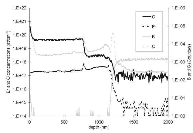
In this project an erbium containing silicon film on a waver was produced by an MBE process. The erbium concentration was verified by the used sources with different Er-content. The results of different sources and different parameters were determined. The concentrations of O and Er were determined by the use of standards. The C and B content were not quantified, because only the relative differences of the samples were relevant. Fig. 1 gives an example of the measurements. In this example it is visible that the O concentration is not constant and there is a C contamination on the interfaces.
Fig. 1: SIMS depth profile of an erbium film on silicon. The elements Er and O were quantified by the use of standards, therefore the concentration is given in at/cm3 (left axis). Because for the elements B and C no standards were available only the counts/s are indicated (right axis).
Blue Light-Emitting Electrochemical Cells
Light-emitting diodes based on conjugated polymers (PLEDs) can be realized with high efficiencies over the whole visible range. The most attractive application of PLEDs is their usage in self-emissive flat panel displays [2].
This part reports the investigations of blue light-emitting electrochemical cells (LEC) based on a ladder-type poly(paraphenylene) (m-LPPP). The turn-on voltage of these LECs occurs at 2.7 V and external efficiencies of around 0.3% and a brightness of around 250 cd/m2 at 10 V were obtained with the LECs based on m-LPPP. The phase morphology of the LECs based on m-LPPP can be optimized in a way that LECs with a very fast pulse response in the range of 20 – 30 µs are obtained.
These LECs consist of three layers. The first is an ITO layer (thickness: ~200 nm) as transparent electrode on a glass substrate, the second consists of the conjugated polymer mixed with polyethylenoxide and LiCF3SO3 (ratio 20:10:3, thickness: ~100 nm). As top-electrode usually Al was evaporated on top of the blend film in high vacuum (thickness: ~200 nm).
The SIMS measurements should clarify if there is a separation of the Li+ and the CF3SO3- ions during production and/or the use of the diodes. Ti was of special interest if an enrichment of the ions on the interfaces polymer-ITO and polymer-Al is observable.
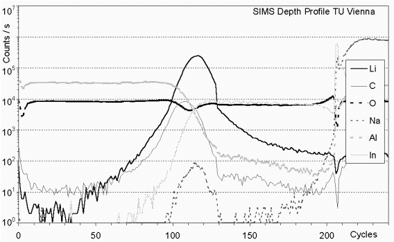
Fig. 2: SIMS depth profile of the LED. Primary ions: O2+. On the right side of the profile the insulating glass substrate is reached. The sample becomes charged at this depth. The Li+ signal is shifted to the right side (relative to the C-peak). This indicates an enrichment of Li at the interface polymer–ITO.
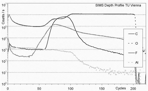
Fig. 3: SIMS depth profile of the LED. Primary ions: Cs+. Due to the atomic-mixing effect the C peak appears wider under Cs bombardment compared to the oxygen profile. The F peak is shifted to the left side relative to the C peak. This indicates an enrichment of F at the interface polymer–Al.
Here only the results of the unused LECs are presented. Due to the different sensitivity of the ions it was necessary to measure the Li+ distribution under oxygen bombardment (see Fig. 2) and the F- and O- ions under cesium bombardment (see Fig. 3). The detection of the S- ion was not possible without the use of high mass resolution, because of the mass interference with O2-. The detection of C as an identifier of the polymer in both measurements allows to fit the depth profiles. This fit is presented in Fig. 4, by way of exception (for SIMS depth profiles) this diagram has a linear y-axis.
In Fig. 4 is clearly visible that there is a enrichment of the ions at the interfaces. This separation takes place already during the manufacturing of the LECs, not by contacting to the supplying voltage.
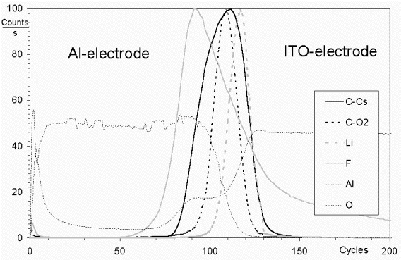
Fig. 4: Normalized intensities from the Cs+- and O2+ measurements. The C peaks from both measurements are printed. For indication of the layers the Al+ and O- signal are given. The maximum of the F- peak is at the interface polymer–Al, the maximum of the Li- peak is at the interface polymer–ITO.
In this project furthermore the influence of different electrodes (Al and Au) was determined. Besides the change of the ions distribution during the use of the LECs were observed.
Conclusion
Microelectronics is a continual challenge for modern material analysis. In many cases improvements of well established analytical methods, like SIMS, are necessary to obtain precise measurement results of the concentration of dopands and trace elements. This knowledge makes the development of new processes and materials possible.
References
[1] W. Jantsch, L. Palmetshofer, "Erbium Related Centres in Silicon" Grundlagen und Technologic elektronischer Bauelemente, Großarl 1995, ISBN 3-901578-01-3
[2] G. Leising, S. Tasch, W. Graupner, "Fundamentals of Electroluminescence in Paraphenylene-Type Conjugated Polymers and Oligomers", Handbook of Conducting Polymers (T. Skotheim ed.), Marcel Dekker New York (1997)
Project Information
Project Manager
Dr. Herbert Hutter
Institute for Analytical Chemistry, Vienna University of Technology
Project Group
|
Last Name |
First Name |
Status |
Remarks |
|
Gritsch |
Martin |
diploma thesis |
|
|
Piplits |
Kurt |
technician |
partial GMe funding |
|
Wolkenstein |
Martin |
dissertation |
Publications in Reviewed Journals
Cooperations