ZnSe/ZnCdSe Quantum Wires on Patterned Substrates
W. Heiß, D. Stifter, G. Prechtl, H. Sitter, W. Jantsch
Institut für Halbleiter- und Festkörperphysik,
Johannes Kepler Universität Linz, A-4040 Linz, Austria
Wide gap II-VI semiconductor compounds are important materials for the fabrication of blue light emitting laser diodes. In this contribution ZnSe/ZnCdSe is used to fabricate quantum well wires. This is achieved by MBE growth on nonplanar GaAs substrates, which are submicrometer gratings with U or V shaped grooves and trapezoidal shaped ridges. In these samples blue luminescence is observed up to room temperature. One dimensional confinement effects are observed by several experiments due to the lateral modulation of the electron gas in the quantum well.
Introduction
The first semiconductor lasers emitting green or blue light are based on wide gap II-VI compounds. In particular ternary ZnCdSe alloys have been used in the active zone of these laser structures [1], [2]. II-VI laser diodes are not available commercially, since the lifetimes of these devices are restricted to several hundred hours. To date, blue light emitting semiconductor lasers based on the GaN material system are more promising for industrial applications. Nevertheless, for several reasons, still lots of efforts are put in the development of laser diodes based on II-VI compound semiconductors.
For III-V semiconductor lasers emitting in the near infrared it was demonstrated already that devices realized from quantum well wire structures possess superior properties, like reduced threshold currents or narrowed emission bandwidths, compared to conventional quantum well lasers [3]. The aim of this work is to fabricate ZnSe/ZnCdSe quantum wire structures using the same technologies as used for the fabrication of laser diodes. ZnSe/ZnCdSe quantum wires showing lateral confinement effects have been achieved in the past by electron beam lithography and wet chemical etching or reactive ion etching. However, these technologies are not commonly used for laser fabrication. In this report we investigate the possibility to obtain II-VI quantum wire structures by MBE-growth on patterned GaAs substrates.
Sample Structures and Results
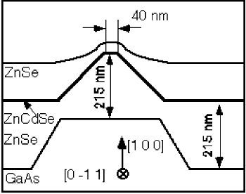
A cross section of a typical sample is sketched in Fig. 1. We use GaAs gratings with submicrometer periods having U-shaped or V-shaped grooves in a crystalline [1` 1 0] direction as substrates. On the substrates ZnSe/ZnCdSe multilayers are grown by molecular beam epitaxy. In particular, ZnSe buffer layers with various thicknesses are grown, followed by a ZnCdSe quantum well, 50 Å thick, and finally by a ZnSe capping layer. A quantum wire is formed due to the dependence of the growth rate on the crystalline orientation. Thus, the lateral width of the quantum wire is determined not only by the period of the substrate, but also by the thickness of the buffer layer. Therefore, wire widths much smaller than the period of the substrate can be achieved.
Fig. 1: Cross section of a typical ZnSe/ZnCdSe quantum well sample.
We have obtained ZnSe/ZnCdSe quantum wire structures, giving intense blue luminescence up to room temperature. TEM images have revealed that the quantum wires are formed on top of the GaAs ridges as sketched in Fig. 1. Depending on the sample structure, luminescence blue shifts up to 10 meV due to the lateral confinement are observed [4]. Furthermore, confinement induced optical anisotropies are observed for several samples [4]. The spatially resolved cathodoluminescence image in Fig. 2 shows clearly a stripe-like intensity distribution of the luminescence confirming the quantum wire nature of our obtained sample structures. Both X-ray investigations and photoluminescence experiments indicate a complex, lattice mismatch induced strain distribution in the quantum structures [5]. Finally, time resolved luminescence experiments reveal a modulation of the exciton-recombination time due to the lateral confinement. This fact opens us the possibility to design the exciton recombination time by nanostructurizing the quantum well samples. This can have important consequences for the improvement of blue light emitting II-VI laser diodes.
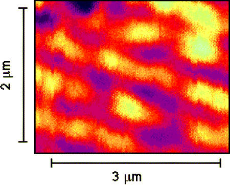
Fig. 2: Spatial resolved cathodoluminescence intensity.
Conclusion
We have fabricated blue light emitting ZnSe/ZnCdSe quantum wires by MBE growth on patterned GaAs substrates. The achieved structures have been investigated by transmission electron microscopy, X-ray measurements and spatial and temporal resolution in photoluminescence experiments. All performed experiments show confinement effects due to a lateral modulation of the two-dimensional electron gas in the quantum well.
Acknowledgments
This work was partially supported by the Austrian Science Foundation (FWF) under contract number P12100-PHY.
References
[1] M. A. Haase, J. Qiu, J. M. DePuydt, H. Cheng: "Blue-green laser diodes", Appl. Phys. Lett., Vol.59, 1272 –1274, 1991
[2] H. Jeon, J. Ding, W. Patterson, A. V. Nurmikko, W. Xie, D. C. Grillo, M. Kobayashi, R. L. Gunshor: "Blue-green injection laser diodes in (Zn,Cd)Se/ZnSe quantum wells", Appl. Phys. Lett., Vol. 67, 3619-3621, 1991
[3] S. Tiwari, J. M. Woodall: "Experimental comparison of strained quantum-wire and quantum-well laser characteristics", Appl. Phys. Lett., Vol. 64, 2211-2213, 1994
[4] W. Heiß, D. Stifter, G. Prechtl, A. Bonanni, H. Sitter, J. Liu, L. Toth, A. Barna: "Lateral confinement in ZnSe/ZnCdSe quantum wells grown on patterned substrates", Appl. Phys. Lett., Vol. 72, 1998, in print
[5] D. Stifter, W. Heiß, A. Bonanni, G. Prechtl, M. Schnid, K. Hingerl, H. Seyringer, H. Sitter, J. Liu, E. Gornik, L. Toth, A. Barna: "Molecular beam epitaxy of ZnSe/ZnCdSe wires on patterned GaAs substrates", J. of Crystal Growth, 1998, in print
Project Information
Project Manager
Univ.-Prof. Dr. Wolfgang Jantsch
Institut für Halbleiter und Festkörperphysik, Johannes Kepler Universität Linz
Project Group
|
Last Name |
First Name |
Status |
Remarks |
|
Heiß |
Wolfgang |
Assistant professor |
|
|
Jantsch |
Wolfgang |
University professor |
|
|
Prechtl |
Gerhard |
Student |
|
|
Sitter |
Helmut |
Associate professor |
|
|
Stifter |
David |
Dissertation |
|
|
Wirtl |
Elisabeth |
Technician |
50% GMe funding |
Publications in Reviewed Journals
Presentations
Doctor’s Theses
Cooperations