UNICHIP Vienna -
ASIC Design with Austrian Universities
N. Kerö, G.R. Cadek, W. Kausel, E. Kowarsch, P. Thorwartl
Institute for General Electrical Engineering and Electronics,
Techn. Univ. Vienna, A-1040 Vienna, Austria
After giving a short overview of the main goals of the UNICHIP initiative and its development over the last years selected activities are presented which have been completed in the last year. Besides two research oriented projects in the area of user programmable logic devices the results of another two ASIC designs for Austrian SMEs are summarized. The report concludes with a description of a LEONARDO project dealing with continued education in Austrian electronic industry.
Introduction
The UNICHIP project was originally proposed in 1987 by the Institute of General EE and Electronics at the Vienna University of Technology. Since its very beginning this national activity was focused on three main topics in the area of the design of digital and analog integrated circuits. Firstly, undergraduate education had to be intensified by means of offering students unrestricted access to state-of-the-art hard- and software electronic design automation (EDA) together with the possibility to actually manufacture selected designs. Secondly, the effective accomplishment of research and advanced development projects should become feasible. Finally, the Austrian industry – mainly small and medium sized enterprises (SMEs) – need to be supported in using new technologies and design methodologies.
All of these aims required continuos investments in design hard- and software tools. Additionally a measurement lab had to be installed enabling the verification on both digital and analog behavior of integrated circuits which have been fabricated in the scope of UNICHIP.
The GMe has funded UNICHIP throughout the past years so we were able to set up and operate a ASIC design facility and thereby achieve every one goal of UNICHIP at least to a certain extent within the first years. The participation in the ESPRIT project Teaching VLSI Design Skills (EUROCHIP) and later on in EUROPRACTICE turned out to be a major breakthrough for UNICHIP. Both of these projects were launched by the European community to accomplish similar goals as UNICHIP but on a pan-European level. Several services are available such as very cheap access to both a variety of EDA tools and to IC prototype manufacturing facilities. Education and academic research word are showing great success and have been pushed to an advanced level comparable to other European universities. In the recent past the SME support activities — by far the most difficult task — have been successful.
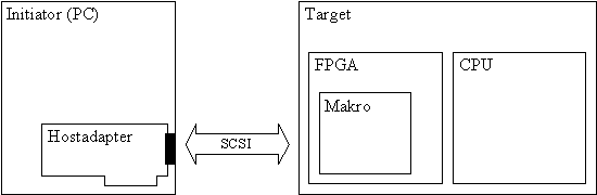
An SCSI-2 Target Marco for FPGAs
In order to speed up the design process of complex digital systems it is common design practice to use macro blocks or modules wherever possible. As long as an FPGA family is selected as the target device these blocks tend to be highly technology dependent. Even worse, families from different FPGA vendors have varying module libraries, thus making it very difficult to migrate a design from one family to another.
Therefore, the aim of this project was to design a re-targetable SCSI-2 macro, to be included in any complex FPGA design. Besides its wide spread usage for the connection of mass storage devices the SCSI bus can handle the attachment of nearly any custom IO device to a standard PC. The necessity to either use (and program) a full fledged SCSI controller or to design one from scratch has been the limiting factor for such applications as shown in Fig. 1.
Fig. 1: Typical SCSI application.
The macro was designed not only by means of VHDL, but with a generic library for the design capture system ViewLogic®. This approach has been chosen because ViewLogic is supported by nearly every FPGA vendor.
The SCSI macro was successfully targeted both to XLINX® and ALTERA® devices. The complexity is roughly 2500 gates which equals 60 CLBs for the logic family XC-4000 from XILINX. A prototype implementation consisting of 4 devices has been tested without any problem with several host adapters.
CULT — Classification of User Programmable Logic Devices with Scaleable Test Structures
The purpose of this project was the search for a new means of classification for User Programmable Logic Devices (UPLD) together with their associated software needed for the design process. In the area of UPLDs are many different concepts and devices all of which are well promoted by their manufacturers as the optimum solution for any digital circuit. Thus an independent classification is of utmost important for the customer, who must select the right architecture for his design problem. All specifications in the official data sheets, like the number of gates or the maximum system frequency, must be corrected by the factor UGF (User Gullibility Factor), depending on the quality of the marketing division.
Existing benchmarks evaluate UPLDs by implementing a set of well defined complex test circuits. The selection of these circuits is a major influence on the results. This project uses very simple identical circuits, so that different UPLD can be compared with each other and also with an easily calculated near optimum result. The different test structures are optimized for measurement of interesting features like system frequency, propagation delay, and utilization of the device.
Entering a certain number of circuits for any different device type seems a rather dull task. A program was developed which can generate all the necessary files in most of the common formats like ViewLogic WIR Files, EDIF or VHDL. Another advantage of this method is the parameterization and scaleability of the benchmark. It is very important to use a well defined design flow to reproduce the results. The single steps of a the design flow are executed automatically with batch files or scripts. The results of the benchmarks are stored in a database.
With this method it is also possible to compare the computational power of different development platforms (PC, SUN). The concepts of this kind of test circuits were verified with all the actual device families from to different vendors (Altera, Xilinx). For the measurement of the propagation delay it is a good idea to use very simple combinatorial circuits like AND gates, exclusive OR gates or multiplexers.
There are three parameters to vary complexity of the test circuit:
The actual maximum propagation delay is measured with a static timing analyzer. If, with an increasing number of output pins, the delay time converges the devices can be called predictable. This is typical for CPLDs in contrast to FPGAs. A comparison of delay time with the number of input pins shows the granularity of the logic cell in a device and the number of logic levels to implement the gate.
On the other hand, for the measurement of the maximum clock frequency the simplest sequential circuit is a serial shift register with various numbers of flip-flops. The results show us the effects of utilization an the maximum possible system frequency. Typically this value is much smaller than the toggle frequency of the D-flip-flops which is the preferred value presented in the data sheets. This test stresses also the partitioning, place and route tools, adjacent flip-flops must be placed as close as possible to each other to achieve the maximum system frequency. This can easily be verified in a floor planner.
The third kind of benchmarks are barrel shifters, which are a combination of the preceding test structures of multiplexers with shift registers. When the number of input pins increases, also the number of logic levels for the combinatorial logic grows and the system frequency decreases rapidly. From these results you can determine the maximum number of logic levels for a given system frequency.
One goal of this work was the demonstration of usefulness of this kind of benchmarks and the development of a set of tools for their evaluation. This is the first type of UPLD benchmark which compares the results to a calculated optimum result derived from theoretical analysis instead of comparing with other UPLD structures.
IVASIC16 — A Binaural Audio Processor ASIC
In a previous project we designed a customized DSP called DAP (Digital Audio Processor) in cooperation with the Austrian company AKG for processing digital audio data to simulate a realistic and natural sound impression, which is achieved by special deep FIR algorithms. The audio processing system was developed by AKG for usage in a professional digital audio environment like recording studios. It comprises a microcontroller, fixed memory, a DAC, a fast static RAM, some glue logic, and finally the ASIC specially designed for this purpose.
We extended the idea of this audio processing system to applications in the area of consumer electronics. For this purpose we had to adapt the concept of the DAP in order to meet the special requirements of a high volume consumer market. We implemented all functions into one chip except for the digital-to-analog conversion and the storage of coefficient data. The goal of this work was to prove the capability of system integration to minimize the overall system cost. Beyond these more economical reasons we wanted to gain detailed experience in using logic synthesis through this industrial design task.
In order to obtain an easily transferable design we decided to use the hardware description language Verilog® for functional design input together with the logic synthesis tool SYNOPSYS®. Placement and routing were accomplished using the CADENCE® software. The design was initially started as a diploma thesis and later carried on as an industrial cooperation together with AKG.
We showed that using system integration offers a large number of benefits. The overall system cost may be reduced by a considerable amount. The usage of VERILOG based functional design entry combined with synthesis using SYNOPSYS showed not only good results but also a speed-up of the design entry task and the capability of fast switching from one ASIC technology to another. The whole design task took about six months. The design has been finished and prototypes have been tested successfully. Volume production is expected to be started within the next months.
Design of a DSP-Based Quad COMBO
Together with our partner company SEMCOTEC we developed a new DSP based four-channel (quad) Combo® device which in turn will be manufactured by National Semiconductor Corp. The main application area of such devices is the telecommunication industry because in digital telephony one Combo® is required for every single subscriber. Currently an advanced integrated circuit production technology permits the integration of the required A/D converter, D/A converter with all the associated filters not only for one subscriber channel but for several channels in a single chip. Devices like that are often referred to as Single/Multi-channel Combos (a combination of COderDECoder + Filter).
The first monolithic Combo devices have become feasible years ago when switched capacitor technology enabled the manufacturing of fully integrated high precision filters together with A/D and D/A converters on the same chip. Devices from this first Combo generation are often referred to as type one Combos and for many good reasons their usage has still not decreased, even today. A type one Combo together with a state of the art monolithic SLIC - or with a conventional transformer SLIC - builds a complete system which can operate a standard voice telephone with all its functionality like ringing, dialing, on-hook/off-hook detection and so on from a standard PCM highway and a digital signaling data carrier. Many thousands of these so called line cards are present in typical digital exchange offices.
The targeted device is a simple, efficient, easy to use, multi-channel Combo. It has to be familiar to the system designers and system manufacturers all over the world who have gained a lot of experience with so called type-one Combos. Therefore all of the features which are not used in low end but high volume applications need not be present. Superior and highly repeatable transmission performance however will distinguish the new multi-channel Combo device from the older and newer analog competitors. By using a state of the art, sub-micron process allowing digital signal processing in combination with over sampling converter techniques most of the disadvantages of current analogue competitors can be avoided.
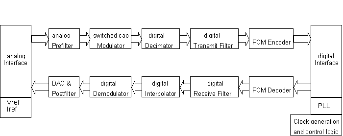
Fig. 2: Global Block Diagram.
The architectural design and the design of the digital blocks were done by the authors while the analog blocks were designed by design engineers from National Semiconductor. The digital design was described in VHDL and extensively simulated with respect to transmission characteristics. Finally, we used SYNOPSYS DesignCompiler for logic synthesis. It took about 15 months from the specification of the devices to the first silicon. The first prototypes were tested successfully. Only some minor design changes have to be applied to adjust the analog behavior. Currently the devices are qualified for production.
LEONARDO Transnational Training Institute
Being a member of the EUROFORM network the institute participates in the LEONARDO project "Transnational Training Institute". The scope of work is the evaluation of the training methodologies employed in SMEs in the area of microelectronics. Together with 7 other partner institutions the efficiency of different approaches such as external or in-house training is analyzed. As a consequence of an overall comparison of the evaluation results in 6 countries the most effective means of training is selected in terms of increased ability to solve given design problems.
EUROFORM is an European network consisting of 60 partners. Within each country a node is responsible for the national coordination of all activities. These nodes are:
In Austria a cooperation with all institutions dealing with training on microelectronics was established. Together with the University Extension Center of the TU Wien and Danube (European Training, Research & Technology) a questionnaire was designed and sent to all known participants of recent training activities. Besides some general information of the structure of the enterprise the questions were focused of the respective activity and the method of distributing the knowledge of the training within the SME.
Finally the SMEs were asked to comment on the type of training they prefer and whether they would accept modern means of presentation (CD-ROM, Internet and the like) and the like.
First evaluations show a strong interest in external training courses with considerable emphasis on hand-on training using EDA-tools and workstations.
Acknowledgments
The Jubiläumsfonds der Österreichischen Nationalbank supported our activities within the project "ASIC-Design Station", the BMwA, the Federal Ministry of Economical affairs, by funding the TMOe (Technologieverbund Mikroelektronik Österreich).
We wish to thank both institutions for their assistance.
Project Information
Project Manager
Dipl.-Ing. Nikolaus Kerö
Vienna University of Technology, Institute for General Electrical Engineering and Electronics
Project Group
|
Last Name |
First Name |
Status |
Remarks |
|
Cadek |
Gerhard |
postdoc |
|
|
Kausel |
Wilfried |
dissertation |
|
|
Kowarsch |
Eduard |
student |
50 % GMe funding |
|
Nachtnebel |
Herbert |
dissertation |
|
|
Pommer |
Heinrich |
dissertation |
|
|
Thorwartl |
Peter |
dissertation |
Publications in Reviewed Journals
Presentations
Doctor’s Theses
Cooperations