Scanning Force Microscopy Investigations of Thermally Grown Oxides on Polysilicon
F. Kuchar, A. Benkitsch
Institut für Physik, Montanuniversität Leoben,
A-8700 Leoben, Austria
The investigations concerned the topography of oxides on silicon and oxygen precipitates in the Si wafers which strongly influence the performance of the oxide layers. In the second case, the size and distribution of oxygen precipitates in Czochralski (CZ) silicon were investigated by Atomic Force Microscopy (AFM). In order to cover the range of interstitial oxygen provided by CZ silicon growth, three ranges of oxygen, 20 – 25, 25 – 30, and 30 – 35 ppma were chosen. The influence of the precipitation behavior on the device performance was determined by measuring the alignment accuracy and the device yield. It could be shown that device performance is not only influenced by the initial oxygen content but also by the size and distribution of oxygen precipitates.
Introduction
We have studied the topography at the transition from the gate oxide to the field oxide. Observed were influences of the nitride etching, thinning of the gate oxide near the bird’s beak, remains of organic resist layers.
To meet the requirements of additional process module integration into deep sub-µm CMOS processes, the properties of the substrate become increasingly important. Therefore AFM investigations have been performed to investigate the size and distribution of oxygen precipitates which are known to directly influence the number of gate oxide defects in MOS transistors.
Since almost all silicon wafers used for the production of VLSI devices are grown by CZ silicon crystal technology, the wafers used for this study were taken from CZ grown ingots. During a CZ process silicon is molten in a quartz or fused silica (SiO2) crucible. A seed crystal is brought into contact with the melt and then slowly withdrawn. Oxygen, an unintended dopant, enters the crystal via melt dissolution of the crucible. The oxygen rich silicon melt rises along the crucible wall, following the thermal convection flow pattern to the surface of the melt, and then to the melt center. There it is drawn towards the crystal by the forced convection induced by the crystal rotation [1].
Only a small fraction (< 5 %) of the dissolved oxygen is incorporated into the growing crystal, because most of the oxygen (> 95 %) evaporates from the free melt surface as silicon monoxide [2]. Therefore the oxygen content of CZ ingots usually ranges from 20 to 33 ppma (old ASTM, 1979).
During the diffusion steps of a CMOS process oxygen precipitates are formed, which causes two advantages. First, the mismatch of the Si and SiO2 lattices and the increase in volume (VSi : VSiO2 = 1 : 2) lead to the emission of dislocations, which getter unintentional contaminants and increase the capability of the wafer to withstand thermal stress. Second, as these precipitates reduce the lifetime of minority carriers, they improve the junction breakdown characteristics [3].
There is a strong interrelationship between crystal growth conditions, grown-in defects, and their impact on device performance. The higher the cooling rate of the crystal, the higher the density of grown-in defects and the smaller their size [4]. Since defects of the lattice are nucleation sites for oxygen, the thermal history of the ingot has a strong influence on the precipitation behavior of the wafers.
Experimental
The radial distortion of 30 N-type wafers (14 – 24 Ohm*cm) with an oxygen content varying from 20 to 35 ppma Oi was measured by determining the current alignment mark position of each chip on the wafer by a laser interferometer after each diffusion step of the CMOS process. To estimate the width of the denuded zone as a function of the oxygen content, a simulation was performed [8].
Additionally one wafer per oxygen range was cleaved and etched with a 50% SECCO etching solution [5], [6] to determine the size and distribution of the oxygen precipitates by an UHV-AFM in contact mode. At the end of the CMOS process, the yield was determined and correlated with the radial distortion of the wafers.
Results
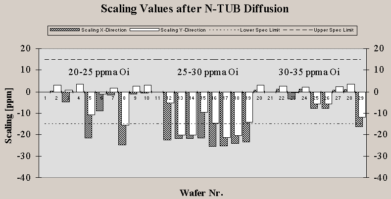
A strong correlation between oxygen content and radial distortion was found (see Fig. 1). But in contrary to what one might expect, the medium oxygen range showed the highest distortion values. Usually the lowest oxygen range should show the highest distortion due to the reduced ability to withstand thermal stress [7]. Further distortion during subsequent diffusion steps doesn’t seem to be influenced by the initial oxygen content (see Fig. 2).
Fig. 1: Wafer scaling after N-TUB Diffusion.
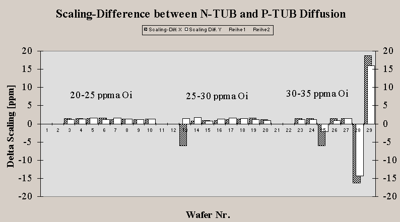
Fig. 2: Scaling difference between N-TUB and P-TUB Diffusion.
The precipitation simulation yielded a denuded zone of 20 µm for wafers with 35 and 70 µm for wafers with 20 ppma Oi, respectively [8], [9], [10].
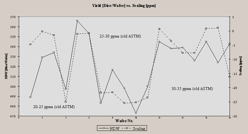
Fig. 3: Overall yield of the device.
The overall wafer yield also corresponds very well to the scaling values of the wafer (Fig. 3). Wafers showing high distortion exhibit few but big oxygen precipitates (Figs. 4 and 5), whereas wafers showing low distortion exhibit many small precipitates (Fig. 6).
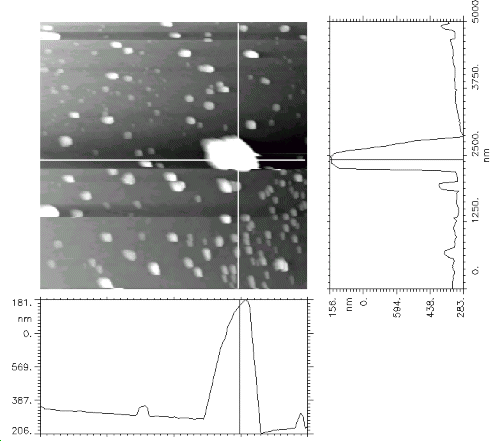
Fig. 4: Cross section of (100) wafer containing 25 – 30 ppma Oi.
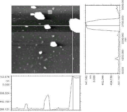
Fig. 5: Cross section of (100) wafer containing 20 – 25 ppma Oi.
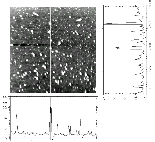
Fig. 6: Cross section of (100) wafer containing 30 – 35 ppma Oi.
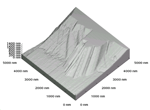
Fig. 7: Step on the cross section of the cleaved wafer (100).
The surface structure exhibits steps and other topographic features (see Fig. 7) due to interaction of the crack with reflected stress waves from the surface of the wafer [11]. These can cause local stress fields at the tip of the crack to be perturbed, thereby altering the trajectory of the crack by kinking it. Other causes of an uneven crack can be load variations as the crack advances. Due to the sufficiently low height of the steps found, no further preparation between cleaving and preferential etching was applied. Apart from that, additional techniques, like polishing, may cause other topographical effects.
Conclusion
The abnormal distortion of some wafers is due to heterogeneous precipitation of oxygen. This is indicated by the different sizes and distributions of the precipitates. Since all wafers were taken from one ingot the different thermal history of each wafer and hence the different densities of intrinsic point defects, which act as nucleation sites, can explain this behavior. In order to reduce the yield loss due to scaling, which reduces the alignment performance of lithography steps, one does not only have to take the oxygen content of the wafers into account but also their thermal history.
References
[1] F. Shimura: "Oxygen in Silicon, Semiconductors and Semimetals", Vol. 42, Academic Press, Inc.
[2] Kyong Min Kim: "Growing Improved Silicon Crystals for VLSI/ULSI Applications", Solid State Technology Vol. 39, No.11, November 1996.
[3] J. Borland, R. Singh: "Improved p-well CMOS latch-up immunity and device performance through intrinsic gettering techniques", technical report.
[4] G. Borionetti, P. Godio, M. Porrini, S. Ilic, Electrochem. Soc. Proceedings Volume 96-13, p.164
[5] F. Secco d’Aragona, J. Elektrochem. Soc. 119, 948 (1972)
[6] H. Rauh: "Wacker’s Atlas for Characterization of Defects in Silicon", Wacker-Chemitronic GmbH, Burghausen, Germany
[7] F. Shimura: "Semiconductor Silicon Crystal Technology", Academic Press, Inc.
[8] M. Cornara: "Simulation of oxygen precipitation", MEMC Electronic Materials, Technical Report, February 199 7
[9] M. Pagani: "Oxygen in Silicon: Nucleation and Precipitation", MEMC Electronic Materials, Technical Report Nr.: GETP0170881104 SS
[10] M. Pagani: "Denuded Zone Formation", MEMC Electronic Materials, Technical Report Nr.: GETP0110881104 SS
[11] A.-B. Chen: "The Mechanical Properties of Semiconductors", Semiconductors and Semimetals, Vol. 37, Academic Press, Inc.
Project Information
Project Manager
Univ.-Prof. Dr. Friedemar Kuchar
Institut für Physik, Montanuniversität Leoben
Project Group
|
Last Name |
First Name |
Status |
Remarks |
|
Benkitsch |
Andreas |
dissertation |
also: process engineer (AMS) |
|
Gold |
Herbert |
dissertation |
|
|
Kuchar |
Friedemar |
university professor |
|
|
Lutz |
Josef |
assistant professor |
(until Sept 1997) |
Publications in Reviewed Journals
Presentations
Cooperations