Preparation of Nano-Structures for Space Applications
G. Stangl, P. Hudek, I. Kostic, F. Rüdenauer, I. Rangelow, K. Riedling, W. Fallmann
Institut für Allgemeine Elektrotechnik und Elektronik,
TU Wien, A-1040 Vienna, Austria
Regular arrays of sub-0.5 µm tips are of increasing interest, for example, as field emitters, calibration structures, or, in our particular case, as collector surfaces for sub-µm dust particles in a space experiment. This contribution describes the preparation of 1 x 1 cm² arrays of micro-columns with a high aspect ratio (10:1) and a diameter in the sub-micrometer range (150 – 300 nm). The process is based upon a chemically amplified novolak resist (CAR), electron beam lithography, and ECR plasma etching.
Introduction
For a space mission of ESA, arrays of sub-µm structures are required as collectors for particles of cosmic dust with 50 – 500 nm diameter. The collected particles will be imaged and classified by atomic force microscopy techniques. It is important that the collector surfaces can collect small high-speed particles with high efficiency and without damage to the particles. They must absorb the kinetic energy of the incoming dust by inelastic processes to avoid reflection of the particles. This can, for example, be achieved by using an array of free-standing columns with a diameter of the order of 0.3 µm and a height in the µm range. An impinging particle may break a number of these columns, thereby incurring an inelastic energy loss that depends on the fracture stress and modulus of the column material and on the column geometry.
The properties of these "collector surfaces" can therefore be tailored to the particular requirements by a variation of the column material and dimensions. By ion etching photoresist column structures into a silicon substrate it is possible to produce arrays of free-standing cones whose fracture energy is considerably lower than that of the resist columns.
Experimental
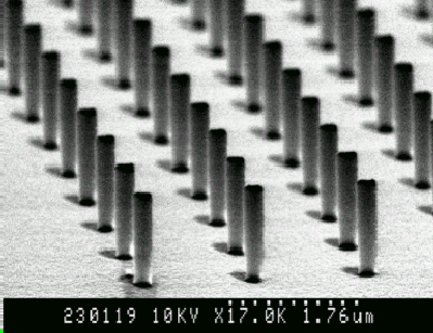
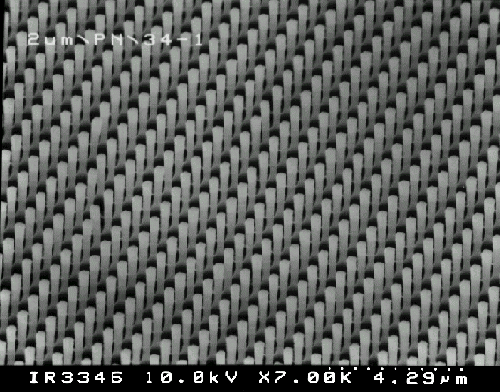
One of the prerequisites for an optimized plasma etching transfer of the structures from the resist layer into an inorganic substrate (for example, silicon or SiO2) is a uniformly structured, relatively thick resist layer with close to perpendicular sidewalls, as shown in Fig. 1.
Fig. 1: Large field (1x1 cm²) array of high-aspect-ratio and high density resist pillars made by using e-beam lithography and chemically amplified resist.
This requires a careful optimization of the deposition, exposure, and of the pre- and post-exposure resist processing. In the experiments reported here, a single film of a three-component negative-toned Novolak CAR (Kalle Hoechst AZ PN 114) has been used [1]. Although the high sensitivity of this resist type makes it very attractive, particularly for electron beam exposure, it causes problems with the control and the uniformity of the critical dimensions. It also requires a precise compensation of proximity effects during electron beam exposure if the pattern dimensions decrease below 0.5 µm, and an optimized resist processing. The most critical factor in resist processing turned out to be the post-exposure delay, which must be less than a few minutes. Although a simulation of the exposure process is indispensable for controlling the proximity effects, the optimization of the entire process heavily depended on experimental work. This is true because the complexity of the three-component resist system and the lack of an exact model of the resist response prohibit a comprehensive simulation.
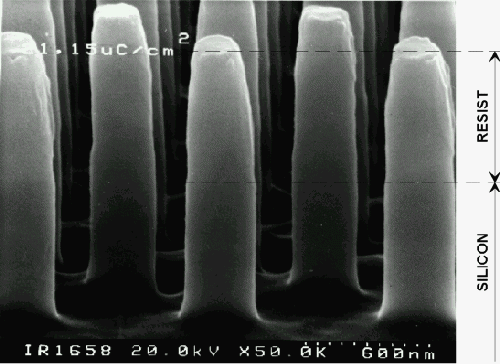
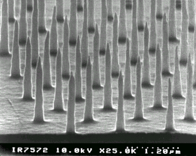
Fig. 2: Large field array of resist pillars transferred into silicon by dry plasma etching (ECR).
The resist column structures may either be directly used as catching structures for dust particles, or they may be transferred into the underlying silicon substrate by means of ECR dry etching (Fig. 2). A careful choice of the etching parameters can allow virtually any shape of the resulting silicon columns (Fig. 3), although the conical shape of Fig. 3(b) appears preferable for the particular purpose. The mechanical behavior and thus the dust collecting capabilities of the structures may also be modified by either removing the resist layer after the etching step or by leaving the mask layer on top of the silicon columns, as shown in Fig. 2.
|
|
|
Fig. 3: Cylindrical pillars (a) and needles (b) prepared in silicon by ECR plasma etching.
Alternative approaches
Other large-area arrays of periodical structures may serve a similar purpose as the columns presented above. Using the same techniques, an array of dust collector boxes may be prepared (Fig. 4).
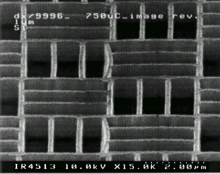
Fig. 4: Array of dust collector boxes prepared by e-beam lithography in chemically amplified resist.
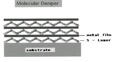
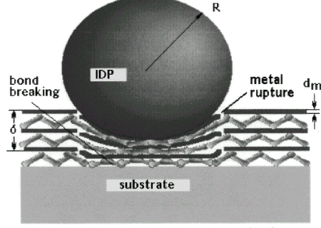
Furthermore, dust collector structures may be "lined" with an energy absorbing sandwich structure consisting of alternate films of crystalline bacterial cell surface proteins ("S"-layers) [2] and evaporated or sputtered metals, e.g., titanium, niobium, or tantalum (Fig. 5(a)). A particle that impinges on such a damping multilayer will either break one or more of the metal films or inelastically deform the S-layer, which results in a smooth absorption of its energy and avoids the loss of particles by reflection (Fig. 5(b)).
|
|
|
Fig. 5: Damping multilayer structure (a) and stopping of a particle (b).
Conclusion
The careful optimization of an electron-beam lithography based single-layer resist process permitted the high aspect ratio patterning of sub-0.5 µm structures in resist with a thickness of up to 5 µm, which is a requirement for a subsequent deep plasma etching. Since the limit for the etching depth in silicon is typically between 2 and 2.5 times the resist thickness, etching depths exceeding 5 µm appear easily feasible with the process presented [3].
Acknowledgments
In addition to the Society for Microelectronics, this work was supported by the Austrian East-West-Funds-Project (OWP-92), and the Erwin Schrödinger Gesellschaft, Institute of Lithographic Research.
References
[1] I. Rangelow, P. Hudek, I. Kostic, Z. Borkiwicz, G. Stangl: "Submicro- and nanometer e-beam lithography and reactive ion etching with single layer chemically amplified negative resist", Microelectronic Eng. 23 (1994) 283.
[2] D. Pum, G. Stangl, C. Sponer, W. Fallmann, U.B. Sleytr: "Deep UV patterning of monolayers of crystalline S-layer protein on silicon surfaces", Biointerfaces 8 (1997) 157 – 162.
[3] P. Hudek, W. Rangelow, I. Kostic, G. Stangl: "Submicro- and nanometer structure fabrication using direct electron-beam writing and reactive ion etching", Electron Technology 28/4 (1996) 251 – 258.
Project Information
Project Manager
A.o.Univ.Prof. Dr. Karl Riedling
Institut für Allgemeine Elektrotechnik und Elektronik, TU Wien
Project Group
|
Last Name |
First Name |
Status |
Remarks |
|
Fallmann |
Wolfgang |
university professor |
|
|
Riedling |
Karl |
associate professor |
|
|
Stangl |
Günther |
technician |
Publications in Reviewed Journals
Presentations
Cooperations