Microstructure Research: Cleanroom Linz
G. Bauer, H. Heinrich, H. Thim
Institut für Halbleiter- und Festkörperphysik and
Institut für Mikroelektronik,
Johannes Kepler Universität Linz, A-4040 Linz, Austria
The activities in the two cleanrooms of the Johannes Kepler Universität Linz are described which were supported in their operation through funds from the Gesellschaft für Mikroelektronik . The main activities are the molecular beam epitaxial growth of Si based heterostructures (Si/SiGe, Si/SiC and Si/SiGe/SiC, Si/SiGeC), the growth of magnetic heterostructures and superlattices like CdTe/CdMnTe, as well as of PbTe/EuTe and the MOCVD growth of GaAs based heterostructures like GaAs/ GaInAs. The lateral patterning of Si/SiGe based heterostructures through holographic lithography as well as through electron beam lithography has been performed and the electronic properties of such structures were investigated by transport, magnetotransport as well as photoluminescence. A standard process module for Si-based heterostructure devices and for the implementation of modulation doped field effect transistors was developed consisting of either 5 or 6 lithographic masks. Furthermore, characterization techniques like UHV-STM AFM were used for studies of the surface morphology of heterostructures and reflectance difference spectroscopy has been implemented as an in situ control process in II-VI molecular beam epitaxy. In addition, experimental results with a 35 GHz Doppler radar unit are reported in this contribution. The measurement setup consists of a RF-front-end, signal conditioning, signal processing and a display unit. The sensitivity of the receiving part has been enhanced by matching a recently developed InGaAs-detector diode with the characteristic impedance of the microstrip transmission line.
Introduction
The GMe funding has made possible research work on various topics carried out by groups from three institutions in the two cleanrooms at the Institut für Halbleiterphysik and at the Institut für Mikroelektronik in Linz. In the following we give short presentations of the results achieved through support of various efforts carried out in these cleanrooms. This concerns the MBE and MOCVD growth of materials, the structural characterization of heterostructures and multilayers through several in situ as well as ex situ methods, the characterization of their electronic and optical properties, and finally the realization of standard process modules for Si based and GaAs based heterostructure devices and the development of high frequency emitters and detectors. Furthermore, research directed to the use of multiquantum well and superlattice structures for infrared detectors and emitters is reported. Detailed information is contained in the cited references, where also all contributors to the investigations are listed.
Experimental
Si-based Process Technologies
(F. Schäffler)
Si Molecular Beam EpitaxyThe activities regarding Si-based heterostructures rely strongly on the quality of the epi-layers, which are grown on-site in our Riber Si-MBE machine. It is located in the clean room of the Semiconductor Physics Group in Linz and utilizes the infrastructure there for substrate preparation and the initial mechanical characterization of the epi-layers by means of a step profiler.
Before introducing the 4" or 5" silicon substrates into the load-lock chamber of our MBE machine, they are chemically pre-cleaned. Since the wafers are usually production-quality substrates from a leading manufacturer, degreasing or other chemical treatments for a removal of organic contaminations are considered detrimental to the quality of the as-delivered substrate surfaces, and therefore avoided, unless a pre-structuring or dicing of the substrates has been performed before growth. Instead, the wafers are either pre-cleaned by a simple dip in diluted (typ. 5 %) HF, or they experience a modified RCA-cleaning procedure, which is very similar to the final treatment applied by the wafer manufacturers after polishing of the substrates. This process, which is named after its inventor, the RCA company, consists of a sequence of two etchants, namely SC1 (NH4OH/H2O2/H2O 1:1:5) and SC2 (HCL/H2O2/H2O 1:1:5), which remove organic and metallic contaminations, respectively. Both SC1 and SC2 are kept in quartz tanks near the boiling point during the agitation period of typically 15 min. The wafers are thoroughly rinsed in DI water after either bath for as long as it takes to bring the DI water resistance to at least 15 MW. Combinations of the RCA clean with one or more HF dips (before and after SC1 and after SC2, or just after SC2) are frequently employed to remove the chemical oxide caused by both SC1 and SC2. The last step before mounting the substrates in the load-lock chamber is always dry blowing in an N2 gas stream.
In 1997 we implemented the RCA cleaning procedure in a flow box next to our MBE machine. Heatable and temperature-controlled quartz tanks capable of adapting up to 6 4" or 5" Si substrates (i.e. the capacity of our load-lock chamber) were acquired from a commercial vendor. The HF tank was home-built and milled from one block of Teflon to avoid any source of contamination that could result from the gaps in a multi-part design. An N2 bubble rinser connected to the DI water supply in our clean room and a N2 blower for drying the wafers complement the cleaning facility.
Because of the decomposition of H2O2 in the RCA baths, and because of hydrocarbon contamination of the HF bath, all chemical agents used in this standard cleaning procedure can only be used once. To keep the cost for the required chemicals as low as possible we therefore reduced the tank volumes to the absolute minimum necessary to completely cover our maximum wafer size of 5". Also, whenever possible (e.g. for calibration wafers or simple epi-tests) we skip the RCA procedure and employ just an HF dip for oxide removal immediately before introducing the wafers into the load-lock chamber. The disadvantage of the HF dip is the concomitant carbon contamination of the interface, which, although it is not electrically active in silicon, is not always acceptable, even if a Si buffer layer is introduced between the interface and the active heterolayers.
Standard Process Module for Si-based DevicesFor an electrical characterization of Si-based heterostructures and for the implementation of modulation-doped field-effect transistors we developed a standard process module consisting of either 5 or 6 lithographic masks (diploma thesis Günther Steinbacher, 1997). Besides an array of field-effect transistors with variable gate length, the layout comprises gated Hall bars and various test structures for process characterization. For example, transmission lines allow to assess the Ohmic contacts, whereas Schottky diodes give access to the Schottky barrier heights an the doping profile near the epi surface.
The process module at this stage is based on the simple mesa technique usually employed for III-V devices, but employs as a Si-specific feature implanted Ohmic contacts. In addition, the process sequence is compatible with a SiO2 or Si3N4 passivation layer, low-temperature deposition of which is planned to be installed in the near future.
The process sequence commences with reactive ion etching (RIE) of alignment marks, which are used for the subsequent lithographic layers. These marks are necessitated by the implanted contact areas, which cannot be used as marks because they become indistinguishable in the optical microscope of the mask aligner after recrystallization. The second lithographic layer defines the contact areas, which are implanted in-house with the photoresist as an implantation mask. After removal of the resist in an O2 plasma and rapid thermal annealing (RTA) of the implanted areas, the same lithography mask is used a second time for lift-off definition of the metallic contact pads. The third lithographic mask defines, per lift-off, the Schottky gates of the transistors, the gated Hall bars and the test Schottky diodes. The fourth mask defines the mesa areas, i.e. it facilitates the lateral electrical separation of the devices and test elements. For this step a negative resist is employed in order to keep the polarity of all mask layers the same. The layout of the mesa-mask is such that the gates of the Hall bars operate as self-aligning mesa masks, i.e., the gate control of the Hall bars is not affected by misalignment. Mesa separation is then accomplished by RIE, with parameters that lead to relatively shallow mesa slopes. These are required by the fifth mask layer, which provides the gate contact pads via a lift-off procedure. To avoid shorts to the underlying active layers induced by ultrasonic contact bonding, the gate contact pads are located in the trenches between mesas, and hence require a connection to the gates on top of the mesas that has to climb up the slope. It is therefore essential to avoid too anisotropic etching of the mesas. The sixth, optional mask layer provides a back contact to the Schottky diodes, which is again located in the plane of the gate contacts. Alternatively, the Schottky diodes are fabricated in a planar fashion, with both contacts in the mesa plane.
The complete process module has been tested, and suitable process parameters for the respective steps have been assigned. Further improvements or fine tuning of these parameters are introduced as experience is gained with the process, or when required by special demands regarding the epi-layer design. For example, contact implantation has to be adapted to the depth of the 2D carrier gas underneath the surface, and it has been recognized that a double implantation, with a shallow projected range for maximum carrier concentration at or near the surface, and a deeper projected range near the 2D channel, is required for optimum contact performance.
The original layout of our process module is based on optical contact lithography. Hence the smallest reproducible structures are 1 µm wide (0.8 µm with some over-exposure). To allow submicron gates of the transistors, additional alignment marks are provided that can be recognized in our e-beam writer. In such a hybrid process all but the gate process are implemented by optical lithography, whereas e-beam lithography and PMMA resist are used for the definition of the gate per lift-off process.
e-Beam LithographyIn 1997 our recently commissioned e-beam writer (Jeol 6400 SEM plus Raith Elphy driver) became operational with demonstrated minimum feature sizes < 100 nm both in additive and subtractive processes (diploma thesis Britta Fünfstück, 1997). The former are used for structuring of metal layers ("lift-off"), whereas the latter are utilized for pattern transfer into the heterostructures via RIE.
So far, our lift-off process is based on a single layer resist, which is only possible by careful determination of the exposure dose. Under optimum conditions, a negative slope of the resist edges develops through overexposure near the substrate by means of secondary electrons generated in the substrate. This procedure has been demonstrated to be working quite well in a situation where a single gate has to be written, which will be the case for implementing the hybrid process mentioned in the preceding subsection. For more complicated structures, or for double gates, where the proximity effect interferes with the required in-depth resist profiling via secondary electrons, more complicated procedures, such as two layer resists, may be required.
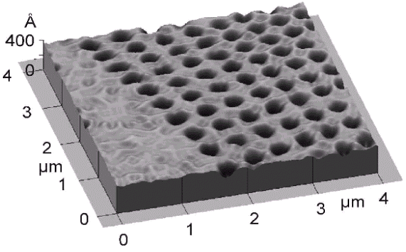
Fig. 1: Anti-dot superlattice defined by e-beam lithography and transferred by RIE into a modulation-doped Si/SiGe heterostructure.
Experiments revealed that structured PMMA is directly useable as a resist for RIE of Si-based heterostructures. By careful adjustment of the RIE parameters in a SF6/CH4 process, we were able to achieve comparable etching rates for Si and PMMA. This is for many purposes sufficient, since usually the RIE process is used for rather shallow trench or mesa etching, which need only be deep enough to interrupt the 2D channel of a highly mobile carrier gas (typically less than 500 Å underneath the surface). As an example, Fig. 1 shows an anti-dot array produced this way with a period of 0.3 µm and an anti-dot diameter of about 150 nm. It was etched into one section of a Hall bar with six potential probes to the depth of the 2D electron gas of a modulation-doped Si/SiGe heterostructure grown in our Riber MBE apparatus. Despite non-optimized RIE parameters, which resulted in reduced carrier mobilities due to RIE damage, we observed a clear commensurability maximum in magnetoresistance measurements. We therefore believe that commensurability oscillations can be used as a sensitive probe for assessing, and optimizing, RIE process parameters with respect to minimum damage.
X-ray Diffraction and Reflectivity from Dry Etched SiGe Wires and Dots
(Y. Zhuang, A.A. Darhuber, J. Stangl, P. Mikulik and G. Bauer)
Si based heterostructures like Si/SiGe have found increasing interest especially because of their potential for application in high frequency circuits. In the SiGe material system the electronic properties depend strongly on the strain status of the layers, i.e. both the band gap as well as the band offsets differ significantly for fully strained or fully relaxed SiGe layers on Si. Any lateral structuring of Si/SiGe heterostructures induces a position dependent elastic relaxation of the misfit strain between the Si and SiGe layers. Therefore for a proper interpretation of optical and electronic properties of laterally patterned SiGe wires and dots, a knowledge of the strain status of the layers is required.
In the case of laterally periodic structures like arrays of wires and dots, the x-ray diffraction (XRD) peaks split into a series of satellites which can be investigated by a mapping of the two-dimensional intensity distribution in the reciprocal space. Information on the geometrical shape of the wire and dot structures is obtained from x-ray reflectivity measurements. Our experimental investigations have shown that strain relaxation in wires and dots is rather complex due to side wall related phenomena, as evidenced by a comparison with finite element calculations.
We have investigated series of dry-etched Si/SiGe quantum wires and dots which were fabricated from MBE grown 10 period Si/SiGe multiquantum well (MQW) structures with Ge contents about 20 %, SiGe layer thickness of about 30 Å and MQW periods of about 200 Å. The wires and dots were defined in the clean room Linz by holographic lithography using an Ar-ion laser set-up and were reactively ion-etched by using a mixture of CH4 and SF6 in an Oxford Plasmalab reactor. Apart from these about 200 nm wide structures, in collaboration with a group from the Nanoelectronics Research Center, Glasgow, also smaller dot structures which had been defined by e-beam lithography, were investigated as well.
With XRD reciprocal space maps of the wire and dot structures close to the (004) and (224) reciprocal lattice points were recorded as shown in Figs. 2 and 3 (10 period Si/Si0.84Ge0.16 MQW structure, dSi = 214 Å, dSiGe = 62 Å, lateral period: D = 440 nm, wire or dot width: 220 nm). The elastic relaxation is deduced from a shift of the diffraction pattern of the etched structures with respect to the substrate peak. The reduction of the in-plane compressive strain after the etching process manifests itself in a shift of the envelope of the wire and dot satellites. The elastic relaxation leads to a decrease of the measured average in-plane strain which is different for wire and dot structures. Due to the uniaxial compression exerted by the Si substrate along the wire axis, the average in-plane elastic relaxation in the wires turns out to be larger than that for the dots.
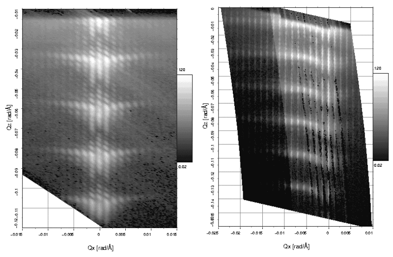
Fig. 2: X-ray diffraction ((004) and (224) reflections) from Si/SiGe reactive ion etched wires.
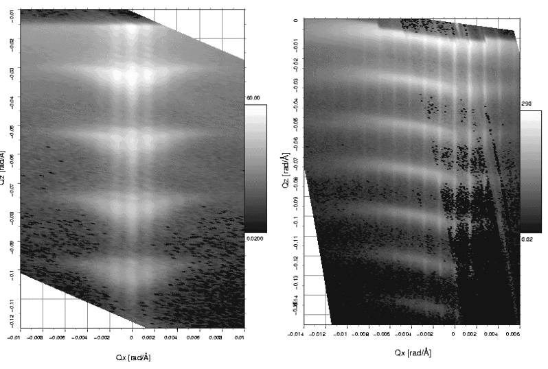
Fig. 3: x-ray diffraction ((004) and (224) reflections from Si/SiGe reactive ion etched dots
This relaxation is defined in relation to the bulk lattice constants of a corresponding SiGe mixed crystal with the same average lattice constant as the MQW structure.
The x-ray reflectivity measurements are sensitive to the grating shape as well as to the interface roughness of the Si/SiGe layers. In the reciprocal space maps recorded around (000), the presence of even order truncation rods reflects side wall imperfections. Furthermore we have observed subsidiary diffuse maxima in between the high intensity wire satellites, which correspond to a period of about 1 µm. Since the Si/SiGe MQW’s were grown on slightly miscut substrates, strain induced step bunching occurred during growth, which leads to terrace widths in the observed length scale. In collaboration with V. Holy, it has been shown that this step-bunching leads to the observed oblique roughness replication in Si/SiGe multilayers grown on miscut (001) Si substrates.
These investigations require in addition to the work done with laboratory x-ray sources experiments at synchrotron sources. We are grateful to DESY, HASYLAB, Hamburg, as well as to ESRF, Grenoble where x-ray diffraction and reflectivity work on these nanostructures has been performed. The MQW samples used for these investigations were grown by S. Zerlauth and F. Schäffler with the Si-Ge-C molecular beam epitaxy growth apparatus in the clean room of the semiconductor physics laboratory, Linz.
Quantum Well Infrared Detectors and Emitters for the Infrared
(M. Helm)
Infrared Detectors on the Basis of Si/SiGe Quantum WellsThe activities on the fabrication and characterization of infrared detectors on the basis of Si/SiGe quantum wells were continued. These detectors, with a spectral response between 4 and 10 µm, are highly sensitive and compatible with silicon technology. The fabrication in the clean room includes several steps of photolithography for the definition of etch and metallization areas, etching of the approximately 100 µm large detector mesas with reactive ion etching, as well as metallization for the formation of electrical contacts using electron beam evaporation. Finally, gold wires are bonded to the contact areas. The characteristics of the best detectors include a peak responsivity (at l = 5 µm) of R = 75 mA/W and a detectivity D* of 2x1010cm÷Hz/W, both at a temperature of T = 77 K.
GaAs/AlGaAs Quantum Cascade EmittersIn collaboration with the Institute for Solid State Electronics at the TU Vienna activities were started to fabricate infrared sources on the basis of intersubband transitions in GaAs/AlGaAs quantum structures. The goal is the realization of a so called quantum cascade laser on the basis of GaAs, similar to the InP based laser, which has already been developed by other laboratories. The fabrication in the clean room again includes several photolithographical steps for the definition of etch and metallization areas, wet-chemical etching of the 100 µm large mesa structures, as well as metallization by e-beam evaporation for the forming of electrical contacts, and gold-wire bonding. Such structures already operate as infrared light emitting diodes, presently at a wavelength of around 7 µm. Eventually, stripe-shaped laser structures will be fabricated by using a suitable waveguide cladding and resonator. Their fabrication technology will require several steps more in the clean room.
Transport and Infrared Absorption in Semiconductor SuperlatticesTransport and infrared absorption investigations were performed in GaAs/AlGaAs superlattices, aiming at the observation of a Wannier-Stark ladder and Bloch oscillations. Standard mesa structures were fabricated using photolithography, wet-chemical etching, metallization, and bonding. The transport measurements show a negative differential resistance, in the infrared measurements the transition from minibands to a Wannier-Stark ladder could be demonstrated through a corresponding absorption line splitting.
Atomic Force and Scanning Tunneling Microscopy
(G. Springholz)
Atomic force microscopy (AFM) is extensively used for the characterization of the epitaxial layers grown in the three different molecular beam epitaxy systems at our institute. For the Si-Ge-C system, the main focus was on the characterization of the cross hatch surface pattern developed during strain relaxation of SiGe layers on Si substrates as a function of Ge content, rate of Ge increase in graded buffer layers and of growth conditions. A considerable part of these measurements were carried out in a research cooperation with the Daimler-Benz research laboratories in Ulm, Germany. For SiC layers, a distinct surface roughening was observed when the carbon content in the layer exceeds a certain critical value. Both observations have important implications for device applications. AFM was used also for defect characterization in strain relaxed SiGe layers where the defects are made visible by selective chemical etchants. For IV-VI semiconductor epitaxial layers, AFM is routinely able to resolve the atomic step structure on the surface and therefore the threading dislocation density in the layers can be directly determined by AFM measurements. AFM is here also used for determination of the size, density and size distribution of self-assembled PbSe quantum dots grown by MBE. Due to the high aspect ratio and highly faceted shape of these quantum dots, the true dot shape could be resolved only when using special ultra-sharp AFM tips. Similar measurements were also made on InAs dots on GaAs and for Ge dots on Si. Atomic force microscopy was also used as a metrology tool for determination of the critical dimensions of semiconductor nanostructures and for the development of sub-micron lithography and pattern transfer processes. We have also performed such measurements for industrial partners, in particular for Sony DAC, Salzburg, for characterization of process modifications in the production of compact discs.
For scanning tunneling microscopy (STM) under ultra-high vacuum conditions, we have designed and set up a new UHV vacuum chamber combined with a small UHV vacuum transfer chamber with which samples prepared by the molecular beam epitaxy systems can be transferred to the separate STM system all under ultra-high vacuum conditions in order to preserve the ultra clean surface structure present after epitaxial growth. With this new system we have investigated the growth mode transitions in strained-layer heteroepitaxy as well as the formation of subsurface defects such as interfacial misfit dislocations formed during lattice-mismatched epitaxial growth. In addition, we have also investigated the surface modifications due to buried 3D islands produced by strained-layer heteroepitaxy in the Stranski-Krastanow growth mode, which are of high interest for direct fabrication of quantum dots. Using spectroscopic techniques we found direct evidence for the electronic confinement in such structures by scanning tunneling microscopy.
As a final activity, we have also started a research activity on the development of sub-micron lithography based on mechanical modifications of thin photo resist layers by scanning force microscopy tips. As a first step we have successfully developed a spin coating process for ultra-thin photo resist layers (thickness of 10 to 30 nm), which will be used as etch mask after modification by the AFM pattern generation.
Molecular Beam Epitaxy of IV-VI Heterostructures
(G. Springholz)
The activities on molecular beam epitaxy on IV-VI semiconductors were concentrated (a) on the direct synthesis of self-assembled quantum dots and (b) on the fabrication of Bragg mirrors for surface emitting lead-salt based optoelectronic devices for the 3 – 5 µm spectral region (mid infrared). Further work included the growth of short period magnetic semiconductor superlattices for the investigation of magnetic interlayer coupling and the preparation of various semiconductor heterostructures for surface studies by scanning tunneling microscopy.
The direct synthesis of self assembled quantum dots by molecular beam epitaxy is based on the general fact that for heteroepitaxy of highly strained layers(lattice-mismatch larger than about 2%), nano-scale three dimensional (3D) islands are spontaneously formed on the surface once a critical layer thickness is exceeded (Stranski-Krastanov growth mode). We have studied here a new materials system for the growth of self-assembled quantum dots, namely, heteroepitaxial growth of -5.4 % lattice-mismatched PbSe on PbTe (111),, materials that have long been used for fabrication of efficient mid-infrared diode lasers. Epitaxial growth was studied using reflection high energy electron diffraction studies in situ during the deposition process and the evolution of surface morphology as a function of layer thickness determined by atomic force microscopy (AFM). We find that when a critical coverage of 1.5 monolayer is exceeded, first chains of PbSe islands are nucleated on the wetting layer, whereas homogenous nucleation sets in at a somewhat larger coverage. Both types of dots exhibit the same pyramidal shape that results from the formation of well defined (100) side facets. As compared to other materials systems (e.g. InAs/GaAs or SiGe/Si), the self-assembled PbSe quantum dots exhibit a remarkably narrow size distribution with relative variation of the dot heights of only ±10 %, which is more than a factor two smaller than for other materials. In addition, this small size variation is found to be independent of layer thickness. These facts indicate the presence of a highly effective mechanism for self-limitation of the island growth, which is obviously related to the highly faceted shape of the PbSe islands. The steep side facets of the pyramidal islnads result in a large stress concentration at the island edges, which produces a strong repulsive potential for the diffusing adatoms deposited on the epitaxial surface. Thus this materials system seems to be very promising for the investigation of zero dimensional quantum structures and for applications for mid-infrared light emitting devices.
With respect to the MIR Bragg mirrors, we have explored the possibilities to fabricate such mirrors by molecular beam epitaxy on the basis of IV-VI materials such that they can be used for IV-VI vertical cavity surface emitting lasers in the 3 – 5 µm region in order to achieve higher operation temperatures for the IV-VI diode lasers. As a starting point we have successfully designed and implemented the fabrication of a Bragg mirror stack consisting of 30 l/4 layer pairs of Pb1-xEuxTe with alternating Eu content of 6 and 1 %, where the latter is realized as a short period PbTe/Pb1-xEuxTe superlattice. Thus, the whole structure consists of more the 1000 individual epitaxial layers and the total thickness is about 15 µm. The reflectivity of the Bragg mirror is tuned to the PbTe energy band gap at 77 K and optical measurements prove a more than 98% efficiency of the fabricated structures. For fabrication of a real laser structure, various wet chemical and plasma etching techniques for mesa definition, as well as the p-type doping of such mirrors was developed.
ZnSe/ZnCdSe Quantum Wire Structures Fabricated by MBE Growth on Patterned GaAs Substrates
(W. Heiss)
We have fabricated blue light emitting quantum wire structures by MBE growth of ZnCdSe/ZnSe quantum wells on patterned GaAs substrates. In particular, we structured (001)-oriented epi-ready GaAs substrates by laser holography using the 457.9 nm line of an Ar+-ion laser. The period of the gratings were chosen to be between 600 nm and 800 nm. Wet chemical etching with a citric acid : H2O2 solution gave an etch rate of about 2 nm/s and resulted in U or V shaped grooves along the crystalline [1 -1 0] direction. Between the grooves, trapezoid-shaped stripes are formed with widths varying between 230 nm and 400 nm. The topology and surface quality of the achieved patterned substrates was checked by scanning electron microscopy and atomic force images. Prior to the growth, the substrates were cleaned and etched in hydrochloric acid for 30 s. This HCl etching procedure strongly improved the crystalline quality of the overgrown ZnSe layers.
On the patterned samples Zn1-xCdxSe/ZnSe multilayer stacks were grown by MBE using elementary Zn, Cd and Se effusion cells. All samples were grown at a substrate temperature of 350 °C in an anion enriched growth regime. Prior to the growth the substrates were thermally cleaned in the UHV chamber at 650 °C until the characteristic reflection high energy electron diffraction (RHEED) pattern became visible. In the RHEED pattern, which exhibits a three dimensional spotty pattern, swallowtail features of the RHEED spots in [1 -1 0] direction reflected the geometry of the {1 1 1} sidewalls of the etched grooves. The growth rate of about 0.1 nm/s was monitored by laser interferometry and by observing the RHEED patterns.
II-VI Compound Heterostructures: Molecular Beam Epitaxy
(H. Sitter)
II-VI compound heterostructures based on ZnSe, ZnTe, CdSe, CdTe, MgSe, MgTe as well as ternary and quaternary compounds were grown on (001) GaAs as well as CdZnTe substrates. In particular, a computer based control system has been installed for choosing and controlling the growth parameters. In situ control is achieved through RHEED, laser interferometry in the visible spectral range, and ex situ control through scanning electron microscopy, transmission electron microscopy, photoluminescence reflectance difference spectroscopy, and x-ray diffraction.
In particular the studies on the doping limits of various II-VI compounds for p-type doping have been investigated. For that purpose two nitrogen plasma sources were developed and realized, one based on DC operation (discharge current) and the other on electron cyclotron resonance (ECR). The plasma parameters were characterized through optical spectroscopy.
Furthermore, RDS has been used for the first time as an in situ control method for the growth of II-VI epilayers in order to characterize surface processes which are related to doping. Using the linear electro-optical effect it turned out to be possible to optimize the doping process and to determine the doping concentration in situ. Using these in situ control methods further improvements in the realization of blue electro-luminescent II-VI heterostructure-diodes were achieved.
A Matched InGaAs Detector Diode for a Ka-Band Radar Front-End
(K. Lübke, G. Haider, C.G. Diskus, A. Stelzer, A.L. Springer, H.W. Thim)
IntroductionThe demand for an increase in data transfer rate and sensor sensitivity raises the interest in devices for millimeter wave applications. The advantage of millimeter-wave sensors is their robustness against environmental factors like dust, water vapor, and noise.
In millimeter-wave systems suited for automotive applications Schottky-barrier diodes are used for detecting and mixing signals because of their high switching speed which results from the unipolar conduction mechanism. III-V semiconductors are the preferred materials because of their higher electron mobility. In this work the design and fabrication procedures of a GaAs FECTED oscillator and a zero bias In0.38Ga1–0.38As-Schottky detector diode for 35 GHz are described.
ExperimentalThe voltage sensitivity of a detector diode is a function of the reverse saturation current. For optimum sensitivity this current has to be in the range of 10–6 A. To achieve this value with GaAs technology at zero bias – which is desirable to keep the circuit as simple as possible – the barrier height must be tailored to 0.22 – 0.25 eV by incorporating indium. With increasing In content the energy gap of the semiconductor is lowered from 1.42 eV (GaAs) to 0.33 eV (InAs). With In0.38Ga0.62As the desired barrier height of the Schottky contact can be adjusted. The diodes have been fabricated using epitaxial layers of GaAs and InGaAs grown by metal organic vapor deposition (MOCVD) on GaAs substrates. Ni/GeAu/Ni/Au films have been evaporated thermally respectively by e-beam and annealed to form ohmic contacts on n-type layers, Ti/Au and Cr/Au were evaporated and used for Schottky contacts. The ohmic contacts have been recessed by wet chemical etching and the connection to the Schottky contact on the top is led over a SiO2 bridge. The etching of the SiO2 has been performed in a reactive ion etching (RIE) reactor.
For reduced bandwidths the sensitivity can be further improved by matching the impedance of the diode to the characteristic impedance of the transmission line. The equivalent circuit of the diode has been deduced from network analyzer measurements. For the frequency range of 34 – 36 GHz a matching circuit consisting of a microstrip stub terminated by a radial stub has been designed and fabricated (Fig. 4).
The patterns for the contact pads, the interconnections and the matching network have been transferred to the substrate using both optical and e-beam lithography.
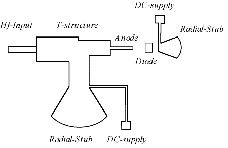
Fig. 4: Schematic illustration of the matching network for the detector diode.
A relatively inexpensive RT/duroidâ 5880 (a trademark of Rogers Corp.) substrate material has been used for the fabrication of the antennas and the 10 dB directional coupler. Each antenna consists of 8 x 8 microstrip patches yielding a beamwidth of 8 degrees.
To guarantee a sufficiently high signal level at the A/D-converter an amplifier with automatic gain control (AGC) is provided. A band-pass filter enhances the quality of the signal by eliminating both noise and low frequency variations. The Doppler signal is converted with a resolution of 16 bit. The signal processing is performed on a DSP-board (Digital Signal Processor) equipped with a SHARC (Super Harvard Architecture Computer, Analog Devices Inc.) signal processor.
ConclusionThe speed sensor has been built and evaluated using an automatic test bench. An accuracy of 0.1 % has been achieved in the case of a corner reflector moving at constant speed. The maximum operational range exceeds 25 m.
AcknowledgmentsThe authors would like to thank M. Hinterreiter and J. Katzenmayer for fabricating and testing the devices. This work was supported by the Austrian Science Foundation (FWF) under Contract number P11424-ÖPY.
References
[1] C. G. Diskus, K. Lübke, A. L. Springer, H. W. Lettenmayr, H. W. Thim: "GaAs Field Effect Controlled Transferred Electron (FECTED) Oscillator MMIC", WOCSDICE ’92
[2] K. Lübke, H. Scheiber and H. Thim: "A Voltage Tunable 35 GHz Monolithic GaAs FECTED oscillator", IEEE Microwave and Guided Wave Letters, (1991) 1, n°2, pp. 35-37
Project Information
Project Manager
Univ.Ass. Dr. Gerhard Brunthaler
Institut für Halbleiter- und Festkörperphysik, Johannes Kepler Universität Linz
Project Group
|
Last Name |
First Name |
Status |
Remarks |
|
Bauer |
Günther |
Full professor |
|
|
Bonanni |
Alberta |
Ph.D. student |
|
|
Brunthaler |
Gerhard |
Univ. Assistent |
|
|
Diskus |
Christian |
Assistant professor |
|
|
Fünfstück |
Britta |
Diploma student |
|
|
Haider |
Gerhard |
Diploma student |
|
|
Heiss |
Wolfgang |
Univ. Assistent |
|
|
Helm |
Manfred |
Assistant professor |
|
|
Hilber |
Wolfgang |
Ph.D. student |
|
|
Hinterreiter |
Marion |
Technician |
|
|
Kainz |
Ursula |
Technician |
|
|
Katzenmayer |
Hans |
Technician |
|
|
Kocher |
Gudrun |
Diploma student |
|
|
Köck |
Franz |
Diploma student |
|
|
Kolmhofer |
Gerald |
Diploma student |
|
|
Kruck |
Peter |
Ph.D. student |
|
|
Lübke |
Kurt |
Univ. Assistent |
|
|
Mikulik |
Petr |
Postdoc |
|
|
Mühlberger |
Michael |
Diploma student |
|
|
Pinczolits |
Michael |
Ph.D. student |
|
|
Rabeder |
Klaus |
Technician |
|
|
Sandersfeld |
Nils |
Ph.D. student |
|
|
Sandner |
Harald |
Diploma student |
|
|
Schäffler |
Friedrich |
Associate professor |
|
|
Schelling |
Christoph |
Ph.D. student |
|
|
Schmid |
Michael |
Ph.D. student |
|
|
Schwarzl |
Thomas |
Diploma student |
|
|
Seyringer |
Heinz |
Ph.D. student |
|
|
Sitter |
Helmut |
Assistant professor |
|
|
Springer |
Andreas |
Univ. Assistent |
|
|
Springholz |
Gunther |
Univ. Assistent |
|
|
Stangl |
Julian |
Ph.D. student |
|
|
Steinbacher |
Günther |
Diploma student |
|
|
Stelzer |
Andreas |
Ph.D. student |
|
|
Stifter |
David |
Ph.D. student |
|
|
Straub |
Hubert |
Ph.D. student |
|
|
Thim |
Hartwig |
Full professor |
|
|
Ueta |
Yukio |
Ph.D. student |
|
|
Wiesauer |
Karin |
Diploma student |
|
|
Wirtl |
Elisabeth |
Technician |
|
|
Wurm |
Ernst |
Technician |
|
|
Zerlauth |
Stefan |
Ph.D. student |
|
|
Zhuang |
Yan |
Ph.D. student |
Publications in Reviewed Journals
Presentations
Patents
Doctor’s Theses
Habilitations
Cooperations