G. Strasser
Institute of Solid State Electronics &
Center of Microstructure Research (MISZ), Techn. Univ. Vienna
A-1040 Vienna, Austria
In this report we describe the main activities in the cleanroom of the MISZ. Not included into this paper are activities directly sponsored by the same society (GMe) which, thus, have their own reports. Since 1995, in the cleanroom of the MISZ state of the art growth of III-V compounds as well as the production of patterned masks used in lithography is done on a regular basis. One of the main research areas of our institute is the preparation and characterization of III-V devices. Therefore the Institute of Solid State Electronics maintains several collaborations with national and international research institutions and companies by providing them with epitaxial layers (III-V-compounds). A second main research topic is the production of micron and sub-micron devices down to nanometer scale. Patterned masks for optical lithography are also provided to different institutions.
During 1997, new equipment was installed in the cleanroom of the MISZ. In detail, an electrochemical CV profiler to measure doping versus thickness profiles was installed and supplied with an additional photovoltaic spectrometer to determine Aluminum concentrations of AlGaAs layers. A UHV system to outgas Knudsen cells and fire pBN-crucibles is under construction. A second spinner including hot plates was installed to spin on photosensitive polyimide. This enables us to produce mesas down to 1 µm with standard optical lithography.
The cleanroom is a necessary tool to manufacture state of the art devices. In the following we will describe all projects within the Institute of Solid State Electronics performed in this cleanroom.
Research Activities
Experimental Investigation on Grating Coupled Twinguide Semiconductor Lasers
(W. Schrenk, N. Finger, A. Köck, M. Haider, M. Socher, E. Gornik)
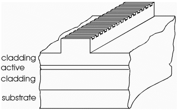
The demand on semiconductor lasers with determined emission wavelength and/or continuous tunable emission wavelength caused different sophisticated laser concepts. The concept to be investigated is a grating coupled twinguide laser. The two waveguides are the active laser waveguide and a passive waveguide on top of a conventional Fabry-Perot laser structure. The two waveguides with different optical properties are coupled via a grating contradirectional only for one determined wavelength. This mechanism acts as a strong wavelength filter in the laser cavity. Therefore the emission wavelength should not drift dramatically with temperature as typical for Fabry-Perot lasers.
Fig. 1: Ridge with grating (schematic).
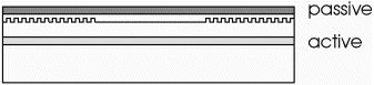
Fig. 2: Schematic view of a ring laser.
Thus, narrow ridge lasers with gratings on the top of the ridge are needed. This problem is solved for ridge widths down to about 1 µm and grating periods of several 100 nm. The second step is to add the passive waveguide on a special laser structure with a thin top cladding and to investigate the filter characteristic of the grating coupled waveguides in respect to the theory. This can be done by a test structure with short grating length. Consequently, a ring laser allows the demonstration of the wavelength selection. It should be possible to reduce the mirror-reflectance of the cleaved or etched mirrors to show laser operation based only on feedback via the passive surface waveguide. The technology for etched laser mirrors is also present. The emission wavelength should be tunable by changing the optical properties of the passive waveguide e.g. via the thickness of the passive waveguide. By adding some asymmetry it should also be possible to force light circulation in only one direction in the ring laser. After showing the coupling mechanism with the ring laser the laser concept must be designed for good efficiency. This would probably be no ring laser but a laser with a grating extended over the full laser length and emission at one antireflection coated laser facet while the other facet could be a metallized mirror.
Fabrication of Vertical-Cavity Surface Emitting Laserdiodes
(T. Maier, W. Smola, G. Strasser, E. Gornik)
With the insertion of a carbon doping source in our MBE system at the beginning of the year we began to grow our first laser structures. To facilitate the characterization of the optical and electrical properties of our samples we used a high-quality GaAs/AlGaAs-DH laser structure received from an external source as a laboratory standard. This structure was grown five times, both LED and broad-area laserdiodes were fabricated, and compared to the standard-devices. The increasing cleanness of the MBE system and optimization of the doping levels brought a continuous improvement. Sample #4 was the first to show laser operation, sample #5 displayed thresholds and efficiencies that were at least equal to our standard sample (Fig. 3).
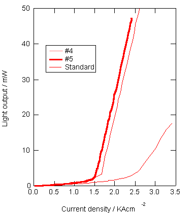
Fig. 3: LI- characteristics of our first broad-area laser diodes compared to a standard device.
The VCSEL structures were grown on n-doped substrates and comprised an n-doped AlGaAs/AlAs bragg-mirror and a DH-GaAs/AlGaAs diode as an active layer. The top mirror was deposited after MBE growth by PECVD and consisted of typically 11 pairs of SiO/SiN. This technique allows a much higher flexibility in the fabrication of the VCSELs compared to the usual all-epitaxial structures, especially the possibility of a post-growth tuning of the resonator to obtain perfect matching of the laser mode and the gain peak.
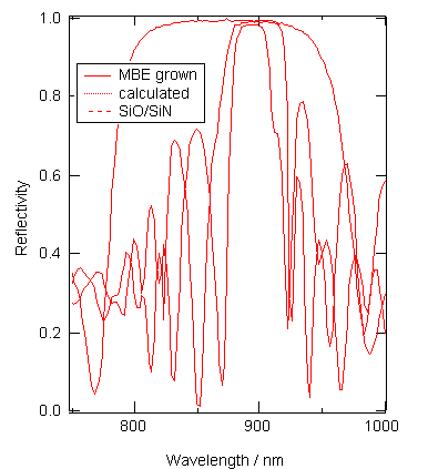
Fig. 4: Reflectivity of an MBE grown VCSEL-structure and that of the SiO/SiN top-mirror.
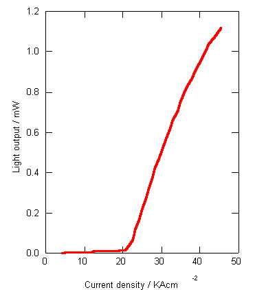
Fig. 5: LI-characteristic of a 7 µm diameter VCSEL with the mirrors shown in Fig. 4.
Figure 4 shows the measured reflectivity of a MBE grown structure together with a calculation. The good accordance underlines the high degree of thickness control during MBE growth that has been achieved. Also shown is the measured reflectivity of a dielectric SiO/SiN top-mirror, reaching values of 99 %, thus fulfilling the demands for VCSEL mirrors.Figure 5 shows the LI-plot of a VCSEL with a 7 µm aperture, measured at a repetition rate of 10 KHz and a duty-cycle of 1 %. The lasing wavelength was 870 nm. The high threshold current densities of approximately 20 KAcm-2 are probably due to a poor current spreading in the p-doped contact layers, resulting in a small mode-gain overlap. By optimizing the doping levels in these layers threshold is expected to be further reduced.
Single-Mode and Single-Beam Surface Emitting Laser Diodes in the Visible Regime
(P.O. Kellermann, A. Köck, N. Finger, E. Gornik)
The surface-mode-emission technique (SME) was successfully applied in the visible red wavelength regime to achieve a single-beam emission via the surface with low beam divergence (0.16° ´ 10°) as well as a single-mode emission in AC and in DC operation with a minimum spectral linewidth of 0.07 nm. The highest sidemode-suppression achieved in AC operation is 19 dB (Fig. 6). With the SME concept the characteristics of a horizontal cavity laser diode (wavelength, emission angle) can be adjusted by changing only the surface parameters (waveguide’s optical thickness, grating period). An optimization of these red GaInP/AlGaInP SME laser diodes towards higher surface emitted power and higher sidemode suppression by contradirectional coupling between the surface- and the lasermode is planned. A diversification of the SME concept to the green regime is under progress, but at present the devices suffer from substantial heating.
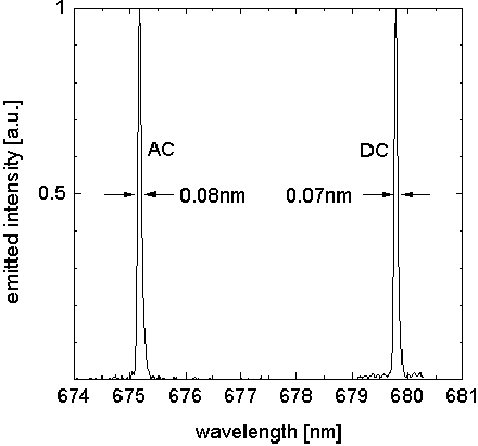
Fig. 6: Single-mode emission spectra of a red SME laser diode in AC operation on the left side and in DC operation on the right side.
The first application of a SME laser diode was realized in high resolution radiography using radiochromic film as dosimeter medium. The readout of the film implements radiochromic film dosimeter near the film’s absorption maximum by using a SME laser diode (675 nm). At 675 nm the effective sensitivity of the film is approximately threefold higher than at 633 nm (helium-neon laser densitometer). Very good accuracy, high spatial resolution, and simple assembly of the readout system has been achieved. The beam profiles of the different collimator helmets of the Leksell Gamma KnifeTM (Elekta Inc., Sweden) installed at the University of Vienna, Department of Neurosurgery, were determined experimentally. Shape and full width at half maximum of the profiles obviously correspond with the computer generated data of the dose planning system. The output factor of the collimators, essential for the application of well defined doses, was checked. The inquiries established an output factor of the 4 mm collimator that lies 9 % ± 1 % lower than the adjusted one.
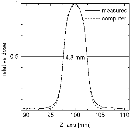
Fig. 7: Measured beam profile of the 4 mm collimator helmet of the Gamma KnifeTM in comparison to the computer generated data.
Investigations on Surface Emitting LEDs by Surface Plasmons and Guided Waves
(S. Gianordoli, A. Köck, E. Gornik)
Excitation and light emission of surface plasmons (SP) represent a method to improve LED performance. To exploit the SP-technique the surface of the investigated LEDs was periodically structured and coated with different metal films. The dependence of the quantum efficiency (QE) and the radiation behavior on the thickness of different metal films (Au, Ag, Al) on cross and hexagonal gratings were investigated. The lowest beam divergence was obtained from a 40 nm thick Ag film on a hexagonal grating and is 17°. The QE for this LED is only 0.22 % due to the reflection of the Au film back into the substrate. The QE without a metal film is 1.4 % to 1.44 %. In addition, photoresist (PR) was spin coated on the metal to stimulate also waveguide modes to increase the QE. The beam divergence broadened but the QE increased to a maximum of 1.37 % for a hexagonal grating with 10 nm thick Au and a 250 nm thick PR-film. In the slope of -30° to 30° the QE is 1 % higher than without metal and PR.
To cancel the decrease of the QE due to the metal backscattering a Bragg-mirror has to be integrated on the substrate side of the LEDs. Together with an optimization of the PR thickness the QE also can be increased.
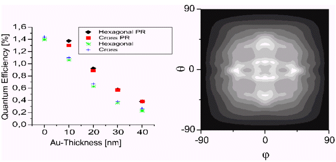
Fig. 8: Quantum efficiency as a function of gold thickness; the right side shows a far field pattern of the LED.
Time Resolved Temperature Mapping in Silicon-On-Insulator Smart Power Devices
(N. Seliger, D. Pogany, C. Fürböck, M. Stoisiek, P. Habas, E. Gornik)
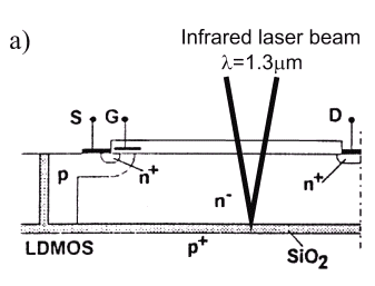
Silicon-On-Insulator (SOI) by Direct Wafer Bonding has become an attractive technique for the fabrication of smart power devices. Self-heating effects in such structures are, however, more critical compared to bulk devices due to a reduced heat removal across the buried and trench oxides. We have developed an optical interferometer technique which allows measurements of the transient temperature variations inside and outside the SOI well of these devices. The temperature variation in the Si layer is monitored by the intensity change of an infrared laser beam (l = 1.3 µm) which is focused on the device from the top side (Fig. 9a). A homogeneous temperature increase DT in the Si layer of the thickness L causes an increase in the optical thickness ![]() due to the thermooptical effect (dn/dT is the temperature coefficient of the refractive index). Light absorption in the highly doped substrate causes that only the temperature induced variation in the optical thickness of the SOI layer is detected via the reflectivity changes of the Fabry-Perot (F-P) resonator formed by SiO2 passivation layer/Si layer/SiO2 buried oxide/Si substrate (Fig. 9b).
due to the thermooptical effect (dn/dT is the temperature coefficient of the refractive index). Light absorption in the highly doped substrate causes that only the temperature induced variation in the optical thickness of the SOI layer is detected via the reflectivity changes of the Fabry-Perot (F-P) resonator formed by SiO2 passivation layer/Si layer/SiO2 buried oxide/Si substrate (Fig. 9b).
|
|
|
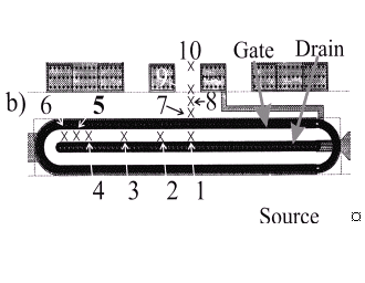
Fig. 9: a) Cross section of LDMOSFET with the laser beam indicated; b) Top view of the device with marked laser beam measurement positions.
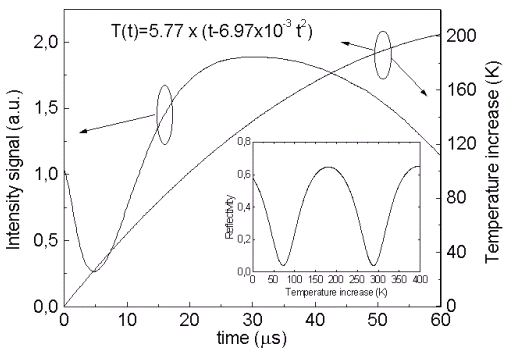
Fig. 10: Intensity signal measured on LDMOSFET and the corresponding temperature function evaluated from the experiment. The inset shows the calculated Fabry-Perot reflectivity as function of temperature for the SiO2/Si/SiO2-multilayer inherent in LDMOSFET.
Heating in the Si active layer is induced by applying short pulses of 20 µs to 100 µs from 0 to 12V to the gate under various drain-to-source biases. From the intensity signals (Fig. 10) measured on different positions we can obtain values for the temperature increase within the device and outside the device.
The temperature from experiment agrees well with results from simulation (Fig. 11).
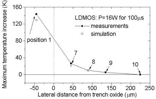
Fig. 11: Peak temperature measured and simulated at different lateral positions (see Fig. 9b) outside the well (Finite Element Simulation by ANSYS).
Internal Characterization of IGBTs Using the Backside Laser Prober Technique
(C. Fürböck, N. Seliger, R. Thalhammer, G. Wachutka, E. Gornik)
Insulated Gate Bipolar Transistors are MOS gated devices which have a high turn-off capability of large current densities in the case of short circuit. Laserprober experiments have been performed on 2nd generation SIEMENS IGBTs. To make the transistor accessible to the laserprober technique the collector metallization on the backside has to be prepared. To provide a vertical bipolar current flow, the IGBT has a thin p-doped layer on the backside (see Fig. 12).
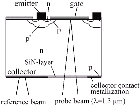
Fig. 12: Principle of backside laser-prober technique applied to the IGBT.
Because of this a mechanical removal of the collector metallization is not possible. A newly developed wet-etching technique provides the possibility to remove parts of the metallization film without etching the silicon. Windows of 70 µm and 90 µm in square are defined, and etched in a two-step process. To avoid multiple reflections within the substrate, an antireflection coating consisting of SiN is deposited in the window area.
In the experiments short circuit case 1 is investigated. A high collector-emitter voltage is applied to the device and the gate is switched to UGE = 15 V for t = 10 µs. To provide sufficient cooling between the pulses a pulse period of 95 ms is chosen. The voltage UCE is varied from 50 to 300 V.
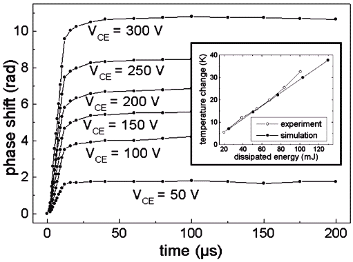
Fig. 13: Transient phase shift under short circuit operation with collector emitter voltages as parameter and a pulse duration of 10 µs. The inset shows the integral temperature change.
In collaboration with the Lehrstuhl für Technische Elektrophysik a simulation of the IGBTs has been performed. The effect of the window in the collector contact metallization on the device behavior was investigated. To distinguish between the signal contribution from the free-carrier and temperature modulation, we made measurements at a low collector-emitter voltage VCE. The contribution from the free carrier concentration is in the range of a few mrad. Hence, it can be neglected at higher power dissipation conditions. Results for this second regime (short circuit operation under high emitter-collector voltage) are shown in Fig. 13. The phase shift is approximately proportional to the total heat dissipated inside the device. From the phase shift an integral temperature change is calculated using the temperature dependence of the refraction index dn/dT = 1,6× 10⁻⁴ K-1. The results are compared with the values from DESSIS simulation, and good agreement has been found.
Optical Testing and Study of Thermal Effects in Semiconductor Devices
(D. Pogany, C. Fürböck, N. Seliger, E. Gornik, S. Kubicek, T. Lalinsky)
A noninvasive infrared laser interferometric technique is used to analyze 0.1 µm test technology NMOSFETs and 0.5 µm technology bipolar junction transistors and PMOSFETs from the back side. The functional state and self-heating effect in the devices are probed by measurements of the optical phase changes caused by the free carrier and thermo-optical effects. The optical signal is studied as a function of bias conditions, device operation frequency and lateral distance from the device (Figs. 14 and 15).
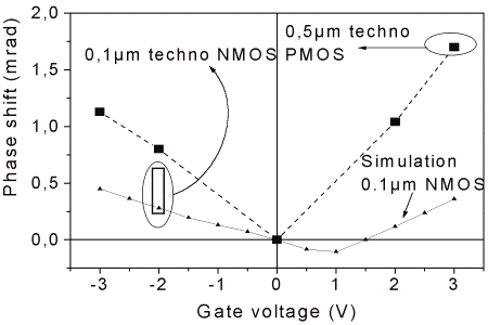
Fig. 14: Phase shift due to the free carrier effect as a function of the gate bias. The dashed line shows the simulation data.
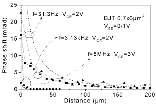
Fig. 15: Phase shift as a function of distance from the emitter of a bipolar transistor. The dashed lines are the simulation results.
Numerical simulation based on the optical characteristic matrix representation for a multilayer system is performed to calculate the free-carrier induced phase shift in MOSFETs. The thermo-optical signal is modeled using a Fourier solution of the heat conduction equation and a simple geometric optic approach. The experiments are in good agreement with the simulations and shows the applicability of the laser method to test VLSI circuits.
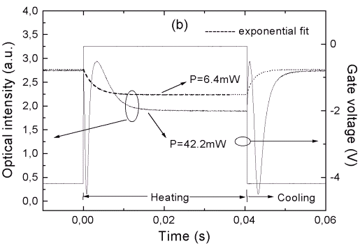
Fig. 16: Time dependencies of optical intensity for two power values. The laser beam is placed in the sensor active area.
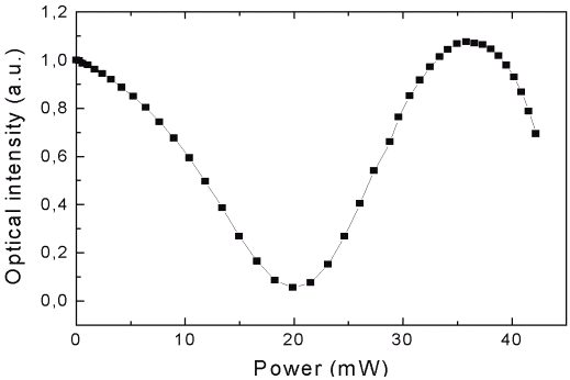
Fig. 17: Optical intensity as a function of dissipated power. The laser beam is positioned on the Schottky diode.
Thermal characteristics of GaAs power sensor microsystem consisting of two cantilever beams are studied by the infrared optical interferometer. Spatial temperature distribution on the cantilever, thermal time constant and power temperature characteristics of the sensor are obtained from time resolved measurements of thermally induced Fabry-Perot optical reflectivity changes (Figs. 16 and 17). A method based on mathematical analysis of the Fabry-Perot intensity peaks is developed to calculate the temperature as a function of time and power. The method is also used to calculate the temperature evolution in smart power devices prepared on silicon-on-insulator (SOI) substrates.
Low Temperature BEEM Studies on InAs/GaAs Heterostructures
(R. Heer, J. Smoliner, G. Ploner, G. Strasser)
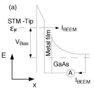
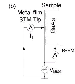
Ballistic Electron Emission Microscopy (BEEM) has been used to perform low temperature studies on MBE grown InAs/GaAs heterostructures. BEEM is a three terminal technique where electrons tunnel between a STM tip (Scanning Tunneling Microscope) and a thin metal-film evaporated on a semiconductor such as Si or GaAs, schematically shown in Fig. 18. The third electrode on the backside of the sample is used to measure the amount of electrons which cross the metal film ballistically and penetrate into the semiconductor.
Originally, BEEM was applied to determine fundamental semiconductor properties such as metal-semiconductor barrier heights, band structure, and hot electron transport effects. Later, BEEM measurements were used to probe subsurface properties of the investigated samples and quantum confined states in a GaAs/AlGaAs double barrier were detected directly. Quantum wires and recently super lattices have also been studied by BEEM.
|
|
|
Fig. 18: Schematically set-up of a BEEM experiment, (a): Band diagram (b): Instrumentation.
BEEM offers the unique possibility of probing subsurface quantum states. Therefore it is important to raise the amount of those electrons which are able to penetrate into the sample, to improve the spectroscopic sensitivity of BEEM.
It is possible to increase the transmission coefficient through the base by more than a factor of 10. The commonly used thin metal film has to be replaced by a MBE grown InAs layer. A passivated InAs cap layer leads to an attenuation length in the regime of 700Å – 900 Å. Compared to a vapor deposited Au film, with an attenuation length of 10 Å, one can see the power of this novel base electrode. In our experiments we could reach the transmission coefficient of 70 Å vapor deposited Au with an 3000 Å InAs cap layer.
Reducing the thickness of the InAs cap layer will lead to a much higher BEEM signal than by the usually used metal film as base electrode, and therefore open a wide spread field of BEEM spectroscopy in the deep subsurface region of samples.
Coherent Plasmons in n-Doped GaAs
(R. Kersting, R. Hoffmann, K. Unterrainer)
One of the most promising sources for pulsed few-cycle THz radiation are coherent plasmons in semiconductors. Due to the large dipole moment of the coherently oscillating charges intense far-infrared emission is expected.
A fundamentally new plasmon excitation is the coherent oscillation of extrinsic electrons in n-doped GaAs. Initially, the extrinsic electrons are confined between the substrate and the surface depletion region (Fig. 19). Femtosecond laser excitation of the GaAs leads to an ultrafast screening of the depletion field. The electrons respond to this field change which starts their coherent oscillation.
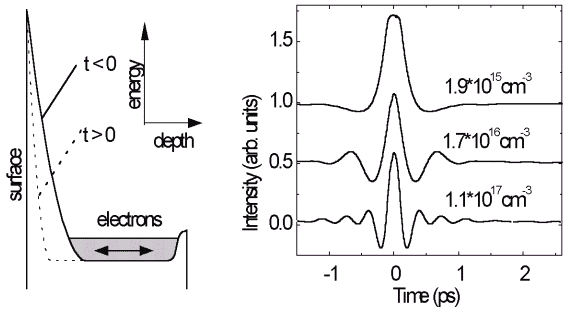
Fig. 19: Left side: Scheme of the excitation process of the coherent electron oscillations. The right side shows correlation data recorded at different doping densities.
Both the excitation and the damping process of the plasmons are investigated in time-resolved experiments on the emitted THz radiation. Figure 19 shows correlation data of the THz pulses. At low doping density an overdamped emission is observed since the oscillation is slower than the damping. According to ![]() the plasma frequency increases with the electron concentration, which leads to well pronounced oscillations at higher doping densities. Since the signals show no dependence on excitation density we conclude that the emission results exclusively from the coherent oscillation of the extrinsic electrons.
the plasma frequency increases with the electron concentration, which leads to well pronounced oscillations at higher doping densities. Since the signals show no dependence on excitation density we conclude that the emission results exclusively from the coherent oscillation of the extrinsic electrons.
In all experiments we observe temporally and spatially coherent THz radiation with intensities of up to 100 nW. However, the pulses are damped out after few oscillations. Temperature dependent measurements show that the damping is due to phonon scattering.
Transient Quantum Coherence of Intersubband Transitions
(R. Kersting, J.N. Heyman, E. Thaller, K. Unterrainer)
Recent technological innovations tend to use quantum coherence phenomena for novel ultrafast devices. One of the most attractive material systems are semiconductor heterostructures due to their huge oscillator strengths and sharp transition linewidths. In our experiments we use electro-magnetic THz pulses to drive electronic intersubband transitions in modulation doped GaAs quantum wells (QWs). The temporal quantum coherence gets directly visible by the time-dependent polarization of the electrons which follows the THz excitation.
The inset of Fig. 20 shows a scheme of the intersubband states in a modulation doped QW. Electrons which are initially located at the lower quantum level are excited by an ultrashort pulse with a center frequency of about 1.5 THz. This THz beam is transmitted through the sample and time-resolved by mixing it with a half-cycle THz pulse and detecting the superposition.
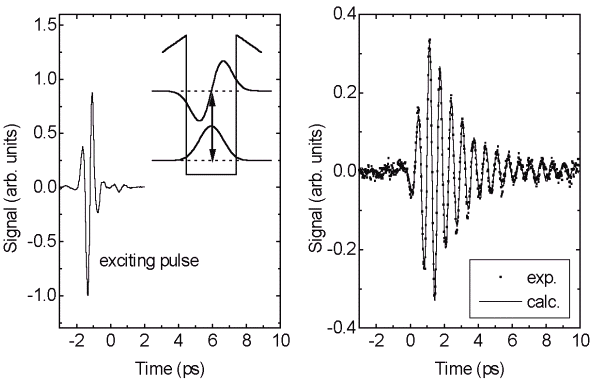
Fig. 20: Left side: The inset is a scheme of the confined electron states (e1, e2) within the QW. The data show the THz pulse exciting the intersubband transition. Right side: Transient response of the electrons when driven by the THz pulse.
Driving the electrons with the few-cycle THz pulse leads to a transient polarization which counteracts the field of the exciting pulse. Modulating the gate bias of the structure and thus the population of the QWs makes the response of the electrons directly visible. The oscillating signal results from the coherent superposition of the states in the first and second subband. During the first ps the exciting THz pulse leads to an increasing amplitude of the electron oscillation. After the driving pulse decayed the amplitude decreases and shows the free induction decay of the collective mode. The solid line is the result of a two-level model calculation. The good agreement enables us to determine the dielectric function of the isolated electron gas in the quantum system.
Far-Infrared Emission from Parabolic Quantum Wells in Magnetic Fields
(R. Zobl, M. Fuchshuber, K. Unterrainer, E. Gornik)
In recent years various types of semiconductor quantum structures have been studied for emission in the THz range. Here the concept of a parabolic potential well and its plasmonic type of FIR emission is studied under lateral current injection. The most interesting feature of parabolically confined potentials is that they absorb and emit radiation only at the bare harmonic oscillator frequency w 0, independent of the number of electrons in the well. This is in accordance with Kohn’s theorem which states that cyclotron resonance absorption is unaffected by electron-electron interaction.
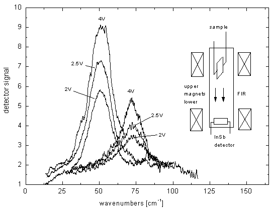
Fig. 21: FIR emission of a parabolic quantum well at 0 T and 4 T. The magnetic field shifts the center frequency by about 20 cm-1. The sample has two top contact pads and a grating coupler.
To investigate the effect of a magnetic field on the FIR emission of the PQW magnetic fields up to 5 T were applied. For a magnetic field direction perpendicular to the layers no CR emission can be observed while the normal intersubband emission almost immediately vanishes even at low magnetic fields. If the magnetic field is applied parallel to the well but perpendicular to the direction of current flow (Fig. 21) CR emission again is not seen whereas a frequency shift of the intersubband radiation is observed starting at magnetic field strengths above 2 T. The shift is attributed to the formation of a strong electric field perpendicular to the well via Hall effect. At 4 T the center frequency of the FIR emission has moved from 50 cm-1 to 70 cm-1 accompanied by a decrease in signal intensity of 50 %. The shifted center frequency position still is independent from the laterally applied electric field and the current flow.
Growth and Characterization of GaAs/AlGaAs Mid-Infrared Emitters
(L. Hvozdara, S. Gianordoli, W. Bichl, G. Strasser, P. Kruck, M. Helm, E. Gornik)
Environmental monitoring, medicine, optical communication and many other areas of technology create a field of application for both, coherent and non-coherent emitters for wavelengths from three to 15 microns.
In the structure depicted in Fig. 22 the intersubband radiative transition (3–2) can be achieved. The energy spacing between levels two and three can be tailored so that the corresponding emitted photon belongs to the mid-infrared band. For the achievement of lasing action there must be a population inversion between the level three and the level two established. An LO-phonon transition between level two and level one secures quick emptying of level two and in this way the condition t(3-2) > t(2-1) for population inversion is satisfied.
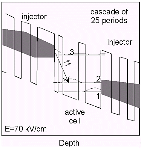
Fig. 22: Calculation of the biased structure. Transition 3–2 is radiative.
I-V characteristics and the photovoltage spectra (Fig. 23) are recorded and the correlation between the self-consistent calculation and the experimental results is found excellent. First attempts to design a laser structure encountered problems with the trade-off between the electrical and the optical properties of the cladding layers.
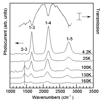
Fig. 23: Typical transmission and photovoltage spectra.
Ballistic Electron Spectroscopy of Semiconductor Quantum Heterostructures
(C. Rauch, G. Strasser, M. Kast, C. Pacher, W. Boxleitner, E. Gornik)
The technique of hot electron spectroscopy is used to measure the transmission properties of resonant tunneling diodes and semiconductor superlattices at different electric fields.
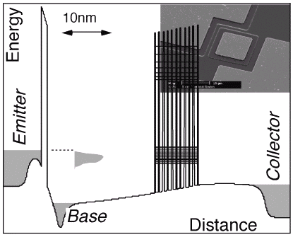
Fig. 24: Conduction band diagram of a hot electron transistor. The inset shows an SEM picture of the device.
A three terminal is used to generate an energy tunable electron beam by a tunneling barrier that passes the superlattice after traversing a thin highly doped n-GaAs base layer and an undoped drift region. The measured collector current reflects the probability of an injected electron to be transmitted through the superlattice. The transmittance of the superlattice can be measured directly at given superlattice bias conditions by varying the injected current independently from the superlattice bias voltage. When a uniform electric field is applied to the superlattice, the quasi-continuous minibands break up into a ladder of discrete Wannier-Stark states. This localization of the electron wave function has direct consequences on the ballistic electron transport. The structures were grown by molecular beam epitaxy on semi-insulating GaAs substrate, the devices were fabricated using standard lithography. An SEM picture and the conduction band diagram of the device is shown in Fig. 24.
Fig. 25 shows the miniband transmission versus applied electric field at 4.2 K. For negative collector bias (decelerating field) the measured current is proportional to the coherent current since electrons that are scattered within the miniband are accelerated back to the base. In case of positive collector bias we measure the coherent current and the additional field induced incoherent current due to Esaki-Tsu like band transport. Since the coherent current is considered to be symmetric for both bias directions, we are able to distinguish between the coherent and incoherent contribution of the collector current.
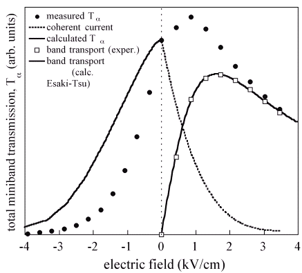
Fig. 25: Miniband transmission versus electric field. Coherent (dashed line) and incoherent current (squares) is present.
These experiments demonstrate for the first time the transition from coherent transport to band like scattering induced transport in a superlattice miniband. Furthermore we have determined the scattering time and the coherence length (lcoh = 80 nm) of the electrons in these superlattices.
By making the length of the superlattice close to the mean free path we believe to match the conditions for Bloch oscillations. The realization of a THz laser based on Bloch oscillation is subject of further experiments.
Project Manager
Dr. Gottfried Strasser
Institut für Festkörperelektronik, Technische Universität Wien
Project Group
|
Last Name |
First Name |
Status |
Remarks |
|
Almeder |
Christian |
student |
|
|
Andok |
Robert |
student |
|
|
Bichl |
Herbert |
student |
|
|
Boxleitner |
Winfried |
Post Doc |
|
|
Bratschitsch |
Rudolf |
student |
|
|
Eder |
Claudia |
dissertation |
50% GMe |
|
Finger |
Norman |
dissertation |
|
|
Fuchshuber |
Michael |
student |
|
|
Fürböck |
Christoph |
dissertation |
|
|
Gianordoli |
Stefan |
dissertation |
|
|
Golshani |
Alireza |
dissertation |
|
|
Gornik |
Erich |
Full Prof. |
|
|
Habas |
Predrag |
Post Doc |
|
|
Haider |
Manfred |
student |
|
|
Hainberger |
Rainer |
dissertation |
|
|
Hauser |
Markus |
Post Doc |
|
|
Heer |
Rudolf |
dissertation |
|
|
Hirner |
Heimo |
student |
|
|
Hobler |
Gerhard |
Assistant Prof. |
|
|
Hoffmann |
Rainer |
student |
|
|
Hvozdara |
Lubos |
dissertation |
|
|
Kast |
Michael |
student |
|
|
Kellermann |
Peer Oliver |
dissertation |
|
|
Kersting |
Roland |
Post Doc |
|
|
Köck |
Anton |
Assistant Prof. |
|
|
Kröll |
Peter |
technician |
|
|
Lampacher |
Peter |
student |
|
|
Langmann |
Gottfried |
technician |
|
|
Liu |
Jian |
student |
|
|
Maier |
Thomas |
dissertation |
|
|
Pacher |
Christoph |
student |
|
|
Patz |
Sybille |
student |
|
|
Ploner |
Guido |
dissertation |
|
|
Pogany |
Dionyz |
guest scientist |
|
|
Prinzinger |
Johannes |
technician |
|
|
Rauch |
Christoph |
dissertation |
|
|
Schenold |
Helmut |
technician |
|
|
Schrenk |
Werner |
dissertation |
|
|
Seliger |
Norbert |
dissertation |
|
|
Smola |
Winfried |
student |
|
|
Smoliner |
Jürgen |
Assistant Prof. |
|
|
Socher |
Michael |
student |
|
|
Strasser |
Gottfried |
Assistant Prof. |
|
|
Thaller |
Edwin |
student |
|
|
Unterrainer |
Karl |
Assistant Prof. |
|
|
Zobl |
Reinhard |
dissertation |
100% GMe |
|
Zotl |
Ernst |
dissertation |
Publications in Reviewed Journals
Presentations
Patents
Doctor’s Theses
Habilitations
Cooperations
Epitaxial Layers:
TU Wien:
Institut für Angewandte u. Technische Physik
Prof. Ebel (AlGaAs layers)
Doz. Schattschneider (GaAs on SiO2)
Doz. Pongratz (Heterostruktures, metallic superlattices)
Atominstitut der österreichischen Universitäten
Prof. Harald Weber
Institut für Analytische Chemie
Prof. Robert Kellner
Universität Wien:
Institut für Physikalische Chemie
Prof. Kauffmann (LTGaAs for high-speed spektroskopy)
Universität Innsbruck:
Institut für Experimentalphysik
Doz. Seidenbusch (Heterostruktures, detectors)
Universität Linz:
Institut für Halbleiterphysik
Prof. Günter Bauer
Doz. Manfred Helm
Universität Leoben
Institut für Physik
Prof. Kuchar (Heterostruktures, 2DEGs)
University of Surrey, UK
Physics Department
Dr. B.N.Murdin
Herriot Watt University, Edinburgh, UK
Prof. C. Pidgeon
Academy of Sciences, Poland
High Pressure Research Center
Prof. Treciakowski (QWs) und Prof. Suski (QW, 2DEGs)
Academy of Sciences, Slowakei
Institut of Physics
Dr. Bartos (DLTS, CV)
Technische Universität Bratislava, Slowakei
Mikroelektronik
Prof. Csabay
Boston College, Boston, Massachusetts, USA
Dep. of Physics
Prof. K.Kempa. Prof. P. Bakshi (FIR emitter)
Prof. D. Broido (SLs)
Georgia State University
Prof. U. Perera (FIR Detectors)