Si/Si1-x-yGexCy Heterostructures
F. Schäffler and G. Bauer
Institut für Halbleiter- und Festkörperphysik, Abteilung für Halbleiterphysik,
Johannes Kepler Universität, A-4040 Linz, Austria
Si/Si1-x-yGexCy heterostructures are promising candidates for all-pseudomorphic n-type hetero-MOSFETs with enhanced electron mobilities that could become an alternative to n-channel Si/SiGe structures on virtual SiGe substrates. We report on the successful optimization of the growth parameters for this novel material combination, which allowed us to overcome problems reported in the literature concerning complete substitutional carbon incorporation into the intrinsically metastable Si1-yCy layers. By concise characterization of the epi-layers with photoluminescence, x-ray diffraction and refraction, and atomic force microscopy, we could also establish a range of growth and annealing conditions that allows a low defect density and a smooth surface morphology. Thus we surpassed in several respects the state-of-the-art quality standards in this material system and achieved a sound material basis that will allow further assessment of this heterosystem regarding future high-performance device applications.
Introduction
It is the outstanding property of Si-based heterostructures to provide the application relevant combination of bandstructure engineering and the compatibility with silicon very-large-scale-integration (VLSI). In the past few years most of the basic properties regarding the lattice mismatched Si/Si1-xGex material combination, and especially the effects of strain on the band offsets and bandgaps, have been investigated [1]. It has been found that the band offset at the interface between a pseudomorphic Si1-xGex layer and a Si substrate occurs almost exclusively in the valence bands, whereas a tensilely strained Si layer is required for the implementation of useful conduction band offsets. By employing proper combinations of pseudomorphic and strain-relaxed epi-layers, both tensile and compressive strains can be custom designed, without sacrificing the important advantages of a Si substrate and the basic compatibility with Si technologies.
By exploiting strain-engineering as an additional degree of freedom, a wide variety of devices structures have been implemented in the Si/ Si1-xGex material system, reaching from heterobipolar transistors (HBT) [2] over p- and n-type modulation-doped field effect transistors (MODFET) [3] to optical detectors in the near infrared, and even light emitters [4]. Nevertheless, so far only the pseudomorphic Si/SiGe HBT has reached production status, whereas other devices with demonstrated superior properties, such as the n-type MODFET, are still restricted to test devices on a laboratory level. The main reason for the much slower development of the MODFET lies in the necessity for strain relaxed Si1-xGex buffer layers. These have successfully been implemented by several research groups [5], [6], [7], but defect and morphology control still require further refinement to make them suited for a production environment.
Ternary Si1-x-yGexCy alloys offer an alternative route to strain-engineering in silicon-based heterostructures, which finally may overcome the problems imposed by relaxed buffer layers: Due to the covalent radii of C and Ge, which are smaller and larger than that of Si, respectively, both compressively and tensilely strained pseudomorphic layers can be implemented by proper adjustment of x and y in the active layers of a heterostructure [8]. However, in contrast to the binary Si1-xGex alloys, which are thermodynamically stable for all compositions x, carbon has almost negligible solid solubility in both Si and Ge, but instead exists in various SiC polytypes. Since strain engineering requires C concentrations of a few atomic percent to provide useful modifications of the band structure [9], non-equilibrium growth conditions at sufficiently low temperatures have to be established. This requires an optimization of the growth parameters to allow sufficiently high C incorporation without excessive degradation of the crystal quality through the undesirable generation of point defects. Also, the surface morphology has to be controlled in order to suppress strain-induced three-dimensional growth.
In the following we report on the recent progress that has been made in Linz regarding the growth and characterization of heterostructures containing ternary Si1-x-yGexCy alloys. The main emphasis in the report period has been put on optimizing the growth conditions to allow a complete substitutional carbon incorporation without sacrificing the structural, morphological, and optical qualities of these layer sequences. These investigations are the most essential prerequisite for any further assessment of the future role Si1-x-yGexCy alloys can play in the field of application-driven band structure engineering.
Experimental
Epitaxial Growth of Si/Si1-yCy Heterostructures
(S. Zerlauth, M. Mühlberger, C. Penn, H. Seyringer, F. Schäffler)
In order to establish and optimize growth conditions for the substitutional incorporation of carbon in concentrations on the order of 1 – 3 at.% we designed and grew a series of six-period Si/Si1-yCy superlattices (SLs) for subsequent characterization by x-ray rocking analyses, photoluminescence (PL), and atomic force microscopy (AFM). The aim of these investigations was to reach a high level of substitutional carbon (to be characterized by the x-ray strain measurements), a low level of electrically or optically active defects (to be characterized by PL measurements), and a smooth surface morphology (to be characterized by AFM experiments).
The two most important parameters for the growth of the thermodynamically metastable compounds, such as Si1-yCy layers, are the growth temperature and the growth rate. Both affect the interplay between surface mobility of the impinging atoms and substitutional incorporation. Low growth temperatures and/or high growth rates always tend to suppress segregation or non-substitutional incorporation, but also lead to defective growth which finally yields an amorphous layer [10]. On the other hand, high growth temperatures and low growth rates move the system closer to thermal equilibrium, which reduces the defect density, but also leads to reduced carbon incorporation or, finally, to stochiometric b-SiC precipitation. Moreover, higher surface mobilities of the impinging atoms will favor three-dimensional (3D) growth, which is frequently observed in strained heterosystems that are allowed to minimize their surface free energy. Under such conditions the reduction of the strain energy via 3D growth has to be larger than the added surface energy introduced by the 3D morphology [11].
In the experiments to be reported here, the growth rate was kept constant at MBE-typical values of around 1 Å/s, and only the growth temperature was varied systematically. To prevent artifacts that might have been introduced by long term fluctuations in the flux of our e-beam carbon source, the complete temperature range to be investigated was frozen into each of our SL samples. To achieve this, the samples were grown under constant Si and C fluxes each, whereas the substrate temperature was systematically increased by 50°C from Si1-yCy layer to Si1-yCy layer over the six periods. This way, each SL contained implicit information on the temperature-dependent incorporation of carbon in the temperature range between 400 and 650 °C. To deduce this information unambiguously, x-ray rocking curves of the SL samples were simulated dynamically with additional input from a set of reference spectra, which came from SLs that were grown at a constant temperature each [16].
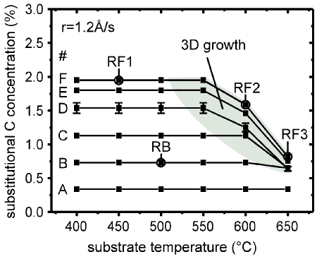
Fig. 1: Carbon incorporation as a function of growth temperature.
The results of these experiments are plotted in Fig. 1. The basic trend is a decrease of the percentage of substitutional carbon both with increasing y and with increasing temperature. In contrast to earlier results of other groups [13], however, we could demonstrate that with reasonably high growth rates (here 1.2 Å/s) complete substitutional carbon incorporation of up to about 2 % is possible at growth temperatures £ 500 °C. Even higher growth temperatures of up to 650 °C are allowed, as long as the desired carbon concentration remains below 1 %.
Beyond the limits established in Fig. 1, the amount of substitutionally incorporated carbon drops drastically with increasing growth temperature (hatched area in Fig. 1). By a combination of RHEED and AFM experiments we found that in this range surface roughness is also strongly increased, whereas the morphology remains basically smooth in the region of complete substitutional incorporation. Additional experiments are required (and planned) to figure out whether increased surface roughness causes the substitution incorporation of carbon to drop, or, vice versa, whether non-substitutional carbon triggers a transition to 3D growth.
Because of the large difference in the covalent radii of Si and C, it was not clear whether a linear interpolation between the lattice constants of Si and diamond (or of Si and SiC) is a good enough approximation even within the quite limited range of substitutional carbon concentrations accessible. Therefore, in cooperation with the group of A.V. Drigo in Padua, who performed resonant backscattering experiments at 5.72 MeV, we studied the variation of the lattice parameter of Si1-yCy layers as a function of the substitutional carbon concentration y. In good agreement with theoretical predictions by Kelires [12], we found a pronounced deviation from Vegard’s rule, which can be as large as 30 %. The reason for that behavior is attributed to the quite significant charge transfer from Si to C, which leads to a faster reduction of the lattice parameter with y than would be expected from a linear scaling of the average bond-length. These new results can be accounted for with a parabolic interpolation scheme, which has to be employed for an accurate determination of the substitutional carbon content via x-ray rocking analyses.
Assessment of Si/Si1-yCy Layers by Photoluminescence
(C. Penn, S. Zerlauth, G. Bauer, F. Schäffler)
The unexpectedly large range of growth parameters that allows substitutional carbon incorporation (Fig. 1 above) makes it possible to grow at sufficiently high substrate temperatures to achieve Si1-yCy layers of high crystal quality with substitutional carbon concentrations of up to at least 2 at. %. In fact, we were able to observe clear bandgap photoluminescence from Si/Si1-yCy SLs within this composition range that allowed us the deduction of the strain-induced band gap narrowing in Si1-yCy layers grown pseudomorphically on Si substrates (dashed line in Fig. 2).
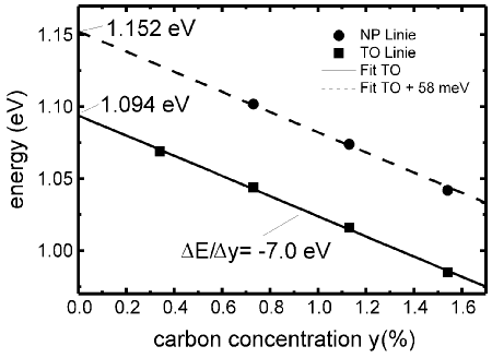
Fig. 2: Band gap variation with increasing substitutional carbon content as derived from photoluminescence measurements.
A linear band gap shrinkage with a slope of -70 meV per percent of substitutional carbon is observed, which leads to a useful band offset of 140 meV at y = 2 % in good agreement with results from other groups [9]. This band gap shrinkage, which is believed to be mainly accommodated by a conduction band offset [9], is almost entirely due to the tensile in-plane strain in a pseudomorphic Si1-yCy layer on a Si substrate, whereas a chemical contribution of the carbon atoms is rather small in the investigated concentration range. At higher concentrations (expected to be beyond 10 at.%) the band gap has to increase again, to finally approach the much larger band gaps of b-SiC (2.2 eV) or even diamond (5.5 eV). However, such large substitutional carbon concentrations are beyond the conceivable limits of metastable, pseudomorphic growth, which renders the question about the composition of the Si1-yCy alloy with the minimum band gap interesting but of little practical relevance.
Photoluminescence spectroscopy is a versatile technique, which not only provides information on the band gaps and the band offsets, but is also a sensitive indicator of the overall crystal quality of the layers, since the density of non-radiative recombination centers has to be small enough to allow the observed phonon- or alloy-disorder-assisted radiative recombination. We have therefore investigated the changes in the PL spectra induced by thermal annealing of the samples, and also as a function of the sample temperature during the PL experiments to get insight into the thermal stability of these intrinsically metastable epi-layers and in the annealing behavior of growth defects.
Three types of samples were grown for these studies, namely Si1-yCy single layers, Si/Si1-yCy multiple quantum wells, and strain compensated Si/Si1-yCy/Si1-xGex superlattices. In the first two types of samples the band offset is almost exclusively restricted to the conduction band, which is energetically lower in the tensilely strained Si1-yCy layers due to a strain splitting of the six-fold degenerate, Si-like conduction band. The situation is analogous to strained Si grown on a relaxed Si1-xGex buffer layer and is therefore of special interest for the implementation of n-type MODFETs. Band alignment in the Si/Si1-yCy/Si1-xGex superlattices, which are interesting for infrared detector applications because of the inherent strain compensation, is more complex: Since the Si1-xGex layers introduce an additional valence band offset, carrier confinement is indirect both in k-space and in real space, with electrons being located in the Si1-yCy layers and holes in the Si1-xGex layers.
At growth temperatures of around 500 °C the as-grown samples of all three types showed well behaved PL signals. There is presently only one other group worldwide that has published PL spectra of comparable quality measured on MBE layers [9]. As an example, Fig. 3 shows the spectrum of a ten-period Si/Si0.989C0.011/Si0.9Ge0.1 superlattice together with a schematic view of the strain-induced band alignment. Two distinct peaks are observed, which originate from band edge recombination in the vicinity of the Si1-yCy/Si1-xGex interface, where the wave functions of electrons and holes have finite overlap. The peak at higher energies, labeled SiC-NP, results from the no-phonon transition, whereas the other peak is its TO phonon replica. A NP transition in an indirect gap material is only possible if symmetry breaking mechanisms are present, such as a heterointerface and/or the statistical fluctuations in a random alloy, which is both the case in our layers. The relative strength of the superlattice related peaks can by judged by comparison with the TO replicas originating from the Si layers and from the substrate. Obviously, the quantum wells very efficiently collect electron-hole pairs from the several µm deep excitation volume, and also maintain long enough lifetimes to allow the observation of radiative recombination. The strength of the bandgap PL signal is therefore an important indicator of the crystal quality, since an excessive amount of defects in the layers and at the heterointerfaces associated with non-radiative recombination would quench the PL signal altogether. This is indeed the case when growth temperatures below 450 °C are employed.
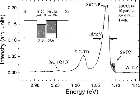
Fig. 3: PL spectrum of a ten-period Si/Si0.989C0.011/Si0.9Ge0.1 superlattice. The dominating signals are the no-phonon (NP) band edge recombination from the quantum well section and its TO-phonon replica. The shaded part of the spectrum is Si-related.
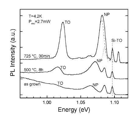
Fig. 4: Evolution of the PL signal of a single Si1-yCy layer for increasing annealing temperatures. Note the blue shift and the line narrowing.
Compared with the well established quantum well luminescence from single Si1-xGex layers [14], the PL signal in Fig. 3 is almost a factor of six broader. Since close to a factor of ten higher Ge concentrations are required to induce the same amount of strain that is provided by a given carbon concentration, the statistical fluctuations of both the well width and the well depth are much more pronounced in the case of a Si1-yCy layer of comparable average strain. In addition, possible composition fluctuations from layer to layer may contribute to the line width from a superlattice. For the investigation of annealing effects we therefore mainly concentrated on single Si1-yCy layers, which were grown thin enough to remain within the critical thickness limitations, but thick enough to suppress quantum confinement effects. Save for the exciton binding energy, this way the true band gap recombination is measured without any necessity for the correction of confinement energies. In addition, cross checks with the multiple quantum well samples confirmed that the annealing behavior is qualitatively the same.
Fig. 4 shows a series of PL measurements from a 100 nm thick Si0.989C0.011 layer which underwent annealing at successively higher temperatures in the range between 500 and 725 °C. There are three main effects associated with annealing: (i) The intensity of the band gap PL signal increases significantly within the range of annealing temperatures shown here. (ii) There is a noticeable blue shift of the PL lines amounting to about 15 meV. (iii) The line width after background subtraction becomes much narrower as the annealing temperature is increased. In fact, the linewidth of 8.4 meV in the topmost curve of Fig. 4 is the narrowest observed to date in any Si1-yCy layer.
Most interesting, the pronounced changes of the PL signal are not associated with a change of the substitutional carbon concentration, as has been checked by x-ray rocking analyses. Only at higher annealing temperatures of >850 °C a loss of substitutional carbon is observed, whereas the PL intensity starts decaying already at about 750 °C.
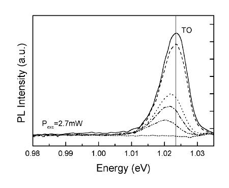
Fig. 5: Red shift of the PL signal with increasing measurement temperature. The TO-phonon replica is plotted here, because it is free of substrate-related signals.
Since changes of the average C concentration can be ruled out, and quantum confinement effects through possible short range diffusion of substitutional carbon can be neglected in the thick layers used here, the development of the PL signal has to have other reasons. To further elucidate these mechanisms, PL measurements of the samples with the highest PL intensity were recorded as a function of the measurement temperature. This is shown in Fig. 5, where the TO-replica of the band gap recombination, which is not affected by spurious signals from the Si substrate, is plotted for measurement temperatures in the range between 4.2 and 20 K. The most striking feature of these measurements, which was confirmed by experiments on the quantum well samples, is a red shift concomitant with a decay of the intensity as the temperature is increased.
A consistent interpretation of the annealing effects and of the red shift with higher measurement temperature can be derived, when assuming that the as-grown samples contain non-radiative recombination centers as well as non-statistical fluctuations of the local, substitutional carbon concentration. The latter may be associated with C2 and C3 molecules, which are observed in the mass spectrum of the carbon molecular beam, and which are tentatively not completely dissociated at the low growth temperatures employed. Based on these assumptions the following effects will occur during annealing:
(i) At low annealing temperatures (middle curve in Fig. 4, 500 °C for 8 h), non-radiative recombination centers associated with growth defects begin to disappear. This leads to an increase of the PL intensity, but only to a minor decrease of the line width.
(ii) At higher annealing temperatures (upper curve in Fig. 4, 725 °C 30 min) a redistribution of carbon on a local scale occurs, which leads to the dissolution of local carbon accumulations, introduced, e.g. by molecular forms of evaporated C. The overall effect is a more homogeneous, statistical distribution of carbon, which causes two effects: First, the PL signal experiences a blue shift, because homogenization of the carbon concentration smears out the local band gap minima in regions of originally enhanced concentration. Second, the line width becomes narrower as the statistical fluctuations become smaller. This interpretation is corroborated by the fact that the ratio between NP signal and TO-replica decreases, which means a reduction of the symmetry-breaking alloy fluctuations.
(iii) Although the fluctuations of the carbon concentration become more homogeneous upon annealing, the remaining alloy is still random. This explains the red shift with increasing measurement temperature, which results from carriers bound to alloy fluctuations, as has been observed in Si1-xGex [15] and other random alloy material systems, too. With increasing temperature the electrons become mobile and establish an equilibrium distribution that preferentially fills the regions with the smallest band gaps. The many available reports in the literature allow the conclusion that a red-shift upon increasing the measurement temperature is a characteristic feature of strongly disturbed alloys with local carrier confinement, which certainly applies to the situation here, because of the large local strain induced by the unusually large difference of the covalent radii of Si and C.
(iv) The layers are thermally stable to beyond 850 °C, with no indications for a change of the average concentration of substitutional carbon. Thus noticeable diffusion of carbon or SiC precipitation requires higher temperatures and should not be a severe limitation for device processing.
Interface Morphology in SiGe/SiC/Si Superlattices
(J. Stangl, A.A. Darhuber, G. Bauer, S. Zerlauth, M. Mühlberger, F. Schäffler)
As has been mentioned above, too high growth temperatures can lead to a roughening of the Si1-yCy layers at the growth front. This may be of crucial influence on the envisaged MODFET applications, because interface roughness scattering can be a mobility limiting mechanism. Now, roughness scattering in a Si1-yCy channel MODFET would occur at the interface between the channel and the subsequently deposited Si spacer layer, and not on a free surface. Because the growth kinetics could modify that interface, it is important to employ a technique that is capable of probing a buried interface.
|
Sample No. |
Periods |
Layer 1 |
Layer 2 |
Layer 3 |
Remark |
|
Z-SGC 312 |
10 |
Si0.9Ge0.1 27Å |
Si0.988C0.012 23Å |
Si 162Å |
surfactant |
|
Z-SGC 314 |
10 |
Si0.989C0.011 21Å |
Si0.89Ge0.11 25Å |
Si 150Å |
|
|
Z-SGC 315 |
10 |
Si0.989C0.011 22Å |
Si0.89Ge0.11 25Å |
Si 149Å |
surfactant |
|
Z-SGC 319 |
10 |
Si0.91Ge0.09 31Å |
Si0.989C0.011 28Å |
Si 191Å |
|
|
M-SGC 575 |
8 |
Si0.79Ge0.21 25Å |
Si0.998C0.002 75Å |
Si 191Å |
|
|
M-SGC 576 |
8 |
Si0.78Ge0.22 25Å |
Si0.991C0.009 42Å |
Si 191Å |
|
|
M-SGC 577 |
8 |
Si0.775Ge0.215 25Å |
- |
Si 191Å |
|
|
M-SGC 580 |
8 |
Si0.805Ge0.195 26Å |
Si0.996C0.004 74Å |
Si 191Å |
Table I: Structural parameters of the investigated samples as obtained from x–ray diffraction and x–ray reflectivity measurements.
This rules out the commonly used and readily available surface sensitive techniques, such as atomic force microscopy or scanning tunneling microscopy. Transmission electron microscopy would be a useful approach, but it is restricted to very small sample areas per micrograph, and, in addition has an in-depth averaging problem that depends sensitively on the quality of sample.
X-ray reflectivity techniques, which are sensitive to changes in the average electron density and thus to chemical composition, can be used instead. In addition, these nondestructive techniques provide information on sample areas which are several mm2 in size, and consequently considerably larger than those which are scanned with scanning probe techniques. However, x-ray reflectivity measurements are not useful for the determination of the strain status of the layers, which requires in addition x-ray diffraction techniques.
Apart from the above mentioned advantages, there are several disadvantages: x-ray reflectivity techniques require the use of synchrotron radiation for sufficient scattered intensity as well as the use of a quite elaborate data analysis. The scattered intensity is recorded in the vicinity of the origin of the reciprocal space (000), and information on interface roughness and its correlation properties are obtained from the analysis of diffusely scattered radiation which accompanies the coherently scattered one.
To investigate the interface morphology and its replication in Si/SiGe/SiC heterostructures, two series of superlattice (SL) samples have been grown by MBE. The first sample series consists of four 10–period Si0.9Ge0.1/Si1-yCy/Si superlattices grown on (001) Si substrates. The growth temperature of all samples was set to 500 °C to ensure fully substitutional incorporation of carbon; the flux rates were typically 1 Å/s. With this series the influence of the layer sequence (SiGe/SiC/Si or SiC/SiGe/Si) and the possible influence of a Sb surfactant was checked. All samples have a nominally 1000 Å thick Si cap on top, as they were also designed for PL–investigations of their neighboring confinement band structure.
The second sample series consisted of four superlattices, where the C content of the Si1-yCy layers was varied, while the SiGe layer composition and thickness as well as the superlattice period were kept constant. The Si1-yCy layer thickness was chosen accordingly to the C content in order to keep the superlattices strain symmetrized. The nominal growth parameters are listed in Table I.
All samples were characterized by (004) XRD rocking scans, and the miscut of the substrates was measured using triple axis diffractometry (TAD): The orientation of the lattice planes was measured for four different azimuths using the (004) Bragg reflection. The surface orientation was measured in the same azimuths by measuring the position of the specularly reflected beam at low incidence angles (typically 0.5°). By this method the miscut can be determined with a precision of about 0.01° in magnitude and 5° in azimuth.
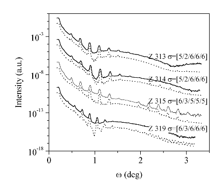
Fig. 6: Scans of the specularly scattered intensity (solid lines) of the first sample series, together with calculations (dotted lines). The corresponding r.m.s. interface roughness values are given in brackets.
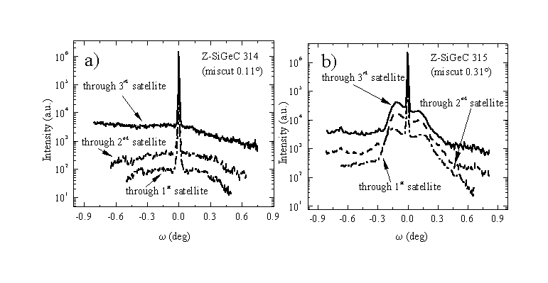
Fig. 7: w–scans through satellite peaks of the specular curve for two samples.
a) for a sample with small miscut, no significant features are observed in the scans; b) for a sample with relatively large miscut, side maxima in the scans are clearly visible.
X–ray reflectivity measurements of the specularly as well as the diffusely scattered intensity were recorded at the Optics beamline (BM5) at the ESRF in Grenoble, France, at the beamlines D4 and RÖMO1 at HASYLAB, DESY, in Hamburg, Germany, and at a laboratory diffractometer in Brno, Czech Republic.
The specular scans of the first sample series (Z-SGC 312 … Z-SGC 319) is shown in Fig. 6, together with calculations using a Parrat-formalism. The resulting r.m.s. roughness values are listed in brackets in the figure. No significant influence of the layer sequence and of the surfactant on the r.m.s. roughness could be detected.
w
–scans of the diffusely scattered intensity revealed different interface morphologies of samples with relatively large miscut (e.g. sample Z-SGC 315 with a miscut of 0.31°) and those with a relatively small miscut (e.g. sample Z-SGC 314 with a miscut of 0.11°), see Fig. 7. For samples with low miscut, no specific structure in the w–scans besides the sharp central peak of the specularly scattered beam could be observed (Fig. 7a). For samples with high miscut strong features in the w–scans could be observed, depending on the azimuth of the measurement. If the scattering plane was perpendicular to the miscut steps of the surface, side maxima in the w–scans were clearly observed (Fig. 7b). From calculations using distorted wave Born approximation, the corresponding length scale of the interface waviness was determined to be approx. 1.7 µm. If the scattering plane is parallel to the miscut steps, only one broad peak in the center of the scan is observed. Furthermore, the vertical correlation length, i.e. the typical decay length for the replication of interface features, is of the order of 2500 Å for the samples with higher miscut, but only 100 to 200Å for samples with small miscut. This clearly indicates that the miscut of the substrate has a significant influence on the growth of the heterostructures.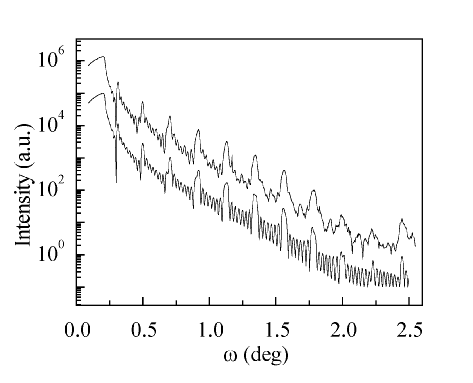
Fig. 8: Scan of the specularly scattered intensity of sample M-SGC 577, together with a simulation.
For the second sample series (M-SGC 575 … M-SGC 580) the interface roughness is slightly smaller: Simulations of the specularly reflected intensity yield an r.m.s. value of 4 Å (see Fig. 8). Virtually no vertical correlation of the interface morphology is observed in these samples, not even in the reference sample M-SGC 577 without SiC interlayers.
The vertical correlation lengths are lower than 100 Å, at least for lateral length scales over 4000Å, which are probed with our experimental setup. We ascribe this effect to the relatively low growth temperature of our samples of only 500 °C.
Conclusion
We have established MBE growth conditions for high-quality Si/Si1-yCy and Si/Si1-yCy/Si1-xGex samples with substitutional carbon concentrations of up to 2 %. Well-behaved PL signals from band edge recombination in the Si1-yCy layers, and at the Si1-yCy/Si1-xGex interface, respectively, have been observed. The quality of the layers improves significantly upon annealing at moderate temperatures of about 725 °C, without affecting the substitutional carbon concentration. At these temperatures annealing mainly reduces the defect density in the layers and leads to a more homogeneous distribution of substitutional carbon. The layers are thermally stable to beyond 850 °C, where we observe first indications for a reduction of the substitutional carbon content. By employing x-ray diffraction and refraction techniques, we were able to gain information on the roughness and replication of buried Si/Si1-yCy interfaces, which is important for interface roughness scattering and almost impossible to gain by other techniques.
Successful growth of carbon-containing, Si-based heterostructures is an important prerequisite for a future implementation of n-type MODFETs with tensilely strained Si1-yCy quantum wells. In a next step the established growth parameters for high-quality Si1-yCy layers on Si will be used as a starting point for the implementation of modulation-doped Si1-yCy quantum wells. This will allow a direct comparison with the established Si-channel MODQWs on strain-relaxed SiGe buffer layers. It will be of special interest to assess the role of alloy scattering in the Si1-yCy wells which directly competes with an elemental Si channel. From such experiments further insight both in the importance of alloy scattering and the future use of Si1-yCy layers can be derived.
Acknowledgments
Close collaboration with Daimler-Benz-Research in Ulm, Germany and with the group of Prof. Drigo in Padua is gratefully acknowledged. The x–ray reflectivity measurements were recorded at the Optics beamline (BM5) at the ESRF in Grenoble, France, at the beamlines D4 and RÖMO1 at HASYLAB, DESY, in Hamburg, Germany, and at a laboratory diffractometer in Brno, Czech Republic. Financial support by the Fonds zur Förderung der wissenschaftlichen Forschung (FWF), and by the Oesterreichische Nationalbank are gratefully acknowledged. C. Penn was partly supported by a scholarship from the Österreichische Akademie der Wissenschaften.
References
[1] for an overview see e.g. E. Kasper and F. Schäffler: "Group IV Elements", Semiconductors and Semimetals, Vol. 33, Academic Press, Boston 1991; chapter 4
[2] for an overview see e.g. A. Gruhle: "Heterobipolar Transistor", Springer Series in Electronics and Photonics; Vol. 52; Springer, Berlin 1994, chapter 4
[3] for an overview see e.g. F. Schäffler: "High-Mobility Si and Ge Structures", Semicond. Sci. Technol., Vol. 12,; 1997; pp. 1515 – 1549
[4] for an overview see e.g. H. Presting, H. Kibbel, M. Jaros, R.M. Turton, U. Menczigar, G. Abstreiter, H.G. Grimmeiss: "Ultrathin SiGe Strained-Layer Superlattices - a Step towards Si Optoelectronics", Semicond. Sci. Technol., Vol. 7, 1992; pp. 1127 –1148
[5] E.A. Fitzgerald, Y.-H. Xie, M.L. Green, D. Brasen, A.R. Kortan, J. Michel, Y.-J. Mii, B.E. Weir, Appl. Phys. Lett.; Vol. 59; 1991; 811 – 813
[6] F.K. LeGoues, B.S. Meyerson, J.F. Morar, Appl. Phys. Lett.;Vol 66; 1991; 2903 – 2905
[7] F. Schäffler, D. Többen, H.-J. Herzog, G. Abstreiter, B. Holländer, Semiconductor Sci. Technol.; Vol. 7; 1992; 260 – 265
[8] K. Eberl, S.S. Iyer, F.K. LeGoues, Appl. Phys. Lett.; Vol. 64; 1994; 739 – 741
[9] K. Brunner, K. Eberl, W. Winter, Phys. Rev. Lett.; Vol. 76; 1996; 303 – 305
[10] H. Jorke, H. Kibbel, F. Schäffler, H.-J. Herzog: "Low Temperature Kinetics of Si(100) MBE Growth", Thin Solid Films; Vol. 183; 1989; 307 – 313
[11] This so called Stranski-Krastanov growth mode is now widely employed for the investigation of self-organization phenomena, which can be useful for the fabrication of zero-dimensional quantum dots.
[12] P.C. Kelires, Phys. Rev. B; Vol. 55; 1997; 8785
[13] H.J. Osten, M. Kim, K. Pressel, P. Zaumseil: "Substitutional vs. interstitial carbon incorporation", J. Appl. Phys.; Vol. 80; 1996; pp. 6711 – 6715
[14] F. Schäffler, M. Wachter, H.-J. Herzog, K. Thonke, R. Sauer, J. Cryst. Growth, Vol. 127; 1993; 411 – 415
[15] L.P. Tilly, P.M. Mooney, J.O. Chu, F.K. LeGoues, Appl. Phys. Lett., Vol. 67; 1995; 2488 – 2490
[16] S. Zerlauth, H. Seyringer, C. Penn, F. Schäffler: "Growth Conditions for Complete Substitutional Carbon Incorporation int Si1-yCy Layers", Appl. Phys. Lett.; Vol. 71; 1997; 3826 – 3828
Project Information
Project Manager
Univ.-Prof. Dr. Friedrich Schäffler
Institut für Halbleiter- und Festkörperphysik, Abt. für Halbleiterphysik, Johannes Kepler Universität Linz
Project Group
|
Last Name |
First Name |
Status |
Remarks |
|
Fünfstück |
Britta |
student |
Diploma Thesis Jan. 98 |
|
Gann |
Rudolf |
student |
|
|
Mühlberger |
Michael |
student |
|
|
Penn |
Christian |
grad. student |
GMe funded since Sep. 97 |
|
Sander |
Harald |
student |
|
|
Schäffler |
Friedrich |
Univ.-Prof. |
|
|
Seyringer |
Heinz |
grad. student |
|
|
Stangl |
Julian |
grad. student |
|
|
Steinbacher |
Günther |
student |
Diploma Thesis Sept. 97 |
|
Zerlauth |
Stefan |
grad.student/post-doc |
Ph.D. Thesis Oct. 97 |
Publications in Reviewed Journals
Presentations
Ph.D. Theses
Cooperations